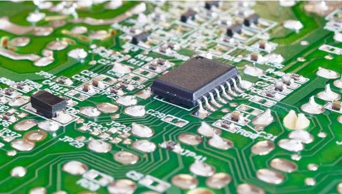
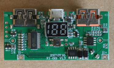
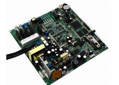
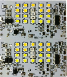
The SMT patch processing process has high patch assembly density and light weight, and it also saves materials, energy and equipment. The processing speed is also very fast and does not require a lot of human resources. The production efficiency is greatly improved, and the production cost is also reduced. Then let's take a look at the advantages and disadvantages of the SMT chip processing process and the production process.
1. The advantages and disadvantages of the SMT chip processing process
1. Advantages of SMT chip processing process:
(1) SMD processing has high assembly density, small size and light weight of electronic products. The volume and weight of SMD components are only about 1/10 of traditional plug-in components. Generally, after SMT is adopted, the volume of electronic products is reduced by 40%- -60%, weight reduction 60%-80%.
(2) High reliability and strong anti-vibration ability. The defect rate of solder joints is low. Good high frequency characteristics. Reduce electromagnetic and radio frequency interference.
(3) It is easy to realize automation, improve production efficiency, and reduce costs by 30%-50%.

(4) Save materials, energy, equipment, manpower, time, etc.
2. Disadvantages of SMT chip processing process
(1) Connection technology issues. (Thermal stress during welding) During soldering, the body of the part is directly exposed to the thermal stress during soldering, and there is a danger of heating several times.
(2) Reliability issues. When assembling to the PCB, the electrode material and solder are used to fix it. The deflection of the buffer PCB without the lead is directly added to the part body, or the soldering part, so the pressure caused by the difference in the amount of solder will cause the part body to break.
(3) PCB testing and rework issues. As the integration of SMT becomes higher and higher, PCB testing becomes more and more difficult, and there are fewer and fewer locations for planting needles. At the same time, the cost of test equipment and rework equipment is not a small amount.
Second, the production process of SMT patch processing
1. Solder paste printing: its function is to print the solder-free paste on the PCB pads to prepare for the soldering of components. The equipment used is a screen printing machine, located at the front end of the SMT production line.
2. Parts placement: its function is to accurately install the surface mount components to the fixed position of the PCB. The equipment used is an SMT placement machine, located behind the screen printing machine in the SMT production line.
3. Oven curing: Its function is to melt the patch glue, so that the surface assembly components and the PCB board are firmly bonded together. The equipment used is a curing oven, located behind the placement machine in the SMT production line.
4. Reflow soldering: Its function is to melt the solder paste, so that the surface assembly components and the PCB board are firmly bonded together. The equipment used is a reflow oven, located behind the placement machine in the SMT production line.
5. AOI optical inspection: its function is to inspect the welding/joining quality and assembly quality of the assembled PCB board. The equipment used is automatic optical inspection (AOI), and the order quantity is usually more than tens of thousands, and the small order quantity is through manual inspection. The location can be configured in a suitable place on the production line according to the needs of the inspection. Some are before reflow soldering/connection, and some are after reflow soldering/connection.
6. Repair: its function is to repair the PCB board that has failed in the detection. The tools used are soldering irons, rework stations, etc. Configured after AOI optical inspection.