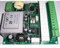
After the PCB board is soldered (including reflow soldering and wave soldering), light green bubbles will appear around individual solder joints. In severe cases, there will be nail-sized bubbles, which not only affects the appearance quality, but also affects the performance in severe cases., Is also one of the problems that often occur in the welding process.
The fundamental reason for the blistering of the solder mask is that there is gas or water vapor between the solder mask and the PCB substrate, where a small amount of gas and water vapor will be entrained in it during different processes. When the soldering high temperature is encountered, the gas expands It will cause the delamination between the solder mask and the PCB substrate. During soldering, the temperature of the pad is relatively high, so bubbles first appear around the pad
The solder mask is blistering.
One of the following reasons can cause the PCB to entrain water vapor:

The PCB processing process often needs to be cleaned and dried before proceeding to the next process. For example, the solder mask should be dried after etching. If the drying temperature is not enough at this time, water vapor will be entrained into the next process, which will cause high temperature during welding. Bubbles appear
The storage environment before PCB processing is not good, and the humidity is too high and the soldering process is not timely dried;
In the wave soldering process, water-containing flux is often used now. If the PCB preheating temperature is not enough, the water vapor in the flux will enter the inside of the PCB substrate along the hole wall of the through hole, and the water vapor first enters around the pad., Bubbles will be generated after welding high temperature.
The solution is:
All links should be strictly controlled. The purchased PCB should be put into the warehouse after inspection. Usually, the PCB should not be blistered after 260 degree Celsius/10s;
PCB should be stored in a ventilated and dry environment, and the storage period should not exceed 6 months;
The PCB should be pre-baked in an oven (120±5) degree Celsius/4h before soldering;
The preheating temperature in wave soldering should be strictly controlled, and it should reach 100 degree Celsius~150 degree Celsius before entering the wave soldering. When using water-containing flux, the preheating temperature should reach 110 degree Celsius~155 degree Celsius to ensure that the water vapor can be completely volatilized.
Causes and solutions of blistering on PCB substrate after soldering
Fingernail-sized bubbles appear after SMA soldering. The main reason is that water vapor is entrained in the PCB substrate, especially for the processing of multilayer boards, which are pre-formed from multilayer epoxy prepregs and then hot pressed. If the storage period of the epoxy resin prepreg is too short, the resin content is not enough, and the pre-drying to remove the water vapor is not clean, it is easy to entrain water vapor after the hot press molding, or the semi-solid film itself contains insufficient glue, and the layer and layer The binding force between the two is not enough, leaving the internal cause of blistering.
In addition, after the PCB was purchased, due to the long storage period and humid storage environment, there was no timely pre-baking before the patch production, so the damp PCB is prone to blistering after the patch.
PCB board blistering
Solution: After the PCB is purchased, it should be checked and accepted before it can be put into the warehouse; the PCB should be pre-baked (125±5) degree Celsius/4h before mounting.