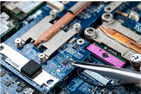
SMT patch processing and assembly method
Technical description of SMT patch processing and assembly method: When SMT patch processing is completed and the current production plan is converted to another patch plan, it is necessary to reprogram various data of the patch machine, replace the supplier, and adjust the substrate conveying mechanism and positioning Operations such as adjusting the patch head and so on are also called reprogramming operations. In the product assembly process, according to customer requirements and assembly equipment conditions, selecting an appropriate assembly method is the main content of its process design. Curved surface assembly technology refers to the placement of thin parts and small parts suitable for surface assembly on the surface of the printed board according to circuit requirements, and the formation of electronic parts assembly technology through welding processes such as heavy flow soldering and wave soldering.
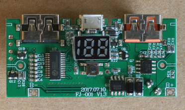
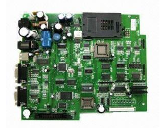
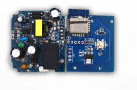
In the traditional THT of the printed circuit board, the parts and solder joints are respectively located on both sides of the printed circuit board, and the solder joints and the parts are on the same side of the panel on the printed circuit board of the SMT chip. In this way, on the SMT chip printed circuit board, the holes are only used to connect the wires on both sides of the circuit board, and their number and diameter are greatly reduced, thereby greatly improving the assembly density of the circuit board. The following is about the finishing of the assembly method in the SMT chip processing technology.

SMT double-sided mixed mode.
One is to disperse SMC/SMD and 17HC through-hole inserts on different surfaces of the PCB for mixed and mixed assembly, but their soldering surface is only one side. The present invention adopts single-sided circuit board and wave soldering (currently double wave soldering is generally adopted) technology, and specifically there are two assembly methods.
SMT single-sided hybrid mode;
SMC/SMD and T.HC can disperse SMC/SMD and T.HC on the same surface, and SMC/SMD can also be dispersed on the same surface of PCB. Double-layer composite welding machine adopts double-sided welding, double wave welding or reflow welding. This assembly method also has the difference between SMC/SMD and sticking first and sticking later. This type of assembly generally uses two types of assembly. PCB. On different sides of SMC/SMD and iFHC, the integrated chip (SMIC) and THC are mounted on the a side of the PCB, and the SMC and small transistor (SOT) are located on the b side.
SMT patch processing penetration weighing principle
The sample of the component to be inspected for SMT chip processing is hung on the sensitive weighing rod, and the inspection sample is placed in the constant temperature melting solder (tin furnace). The combined force of the buoyancy and surface tension of the acting product in the vertical direction is measured by the sensor and recorded by the high-speed characteristic curve. It records the function curve of the force function curve.
Commonness of part pins.
For surface mounting, if the pin passability is not high, it will affect the good contact between the workpiece and the PCB pad.
The standard tolerance for pin coplanarity of flat assembly equipment is 0.1mm.
In other words, the vertical distance between the MAX point of the stitch and the plane formed by the sole of the MIN foot is less than 0.1mm.
Method of measuring the coplanarity of component pins.
Place the component on a plane, measure the value of the MAX sole with a detector, place the component on the optical plane, measure the distance between the non-coplanar pins and the optical plane with a microscope, and use the vision system to automatically detect.
Part performance usually needs to be checked before assembly. Otherwise, it becomes the cost of maintenance and repair.
Use testing equipment to check whether the performance parameters and performance indicators of each component are consistent.
PCB appearance defect inspection.
Alignment of the solder mask with the pad; whether the solder mask has any abnormalities such as impurities, skin, wrinkles, etc.; whether the sign meets the standard; whether the wire width (line width) and spacing meet the standard; whether the multilayer board has peeling, etc.
PCB welding performance test.
Test point: Soldering performance test of PCB pads and electroplated holes.
Test methods: edge dipping test, rotary dipping test, wave dipping test, solder bead test, etc.
Edge immersion test: used to test the weldability of the conductor surface.
Dip the sample (edge) in the flux, take out the excess flux, take it out after the melting bath has melted for a period of time, and evaluate with visual or optical instruments.