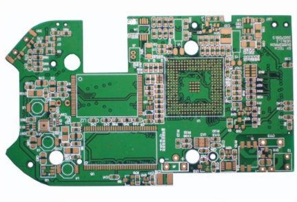
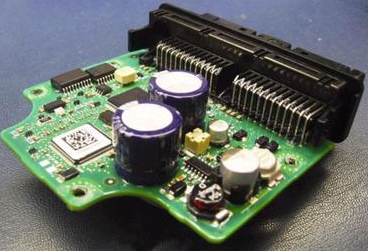
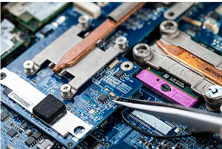
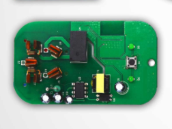
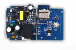
Everyone knows that current electronic products are pursuing miniaturization and portability, which requires the core part of these electronic products, PCB circuit boards, to be smaller and lighter, which also requires the use of smt chip processing technology to achieve. The quality and reliability of solder joints in smt chip processing determines the quality of electronic products. In this regard, Jingbang technicians will introduce the quality and appearance inspection methods of smt patch processing solder joints:
1. The appearance of well-processed solder joints should meet the following points:
1. The surface needs to be complete, smooth and bright, without defects;
2. With good wettability, the edge of the solder joint should be thin, and the wetting angle between the solder and the surface of the pad should be less than 300, and the maximum should not exceed 600;
3. The height of the component should be moderate, and the proper amount of solder and the solder should completely cover the soldering part of the pad and the lead.
2. Contents to be inspected for the appearance of SMT processing:

1. Whether there are any missing components;
2. Whether the components are pasted incorrectly;
3. Whether it will cause a short circuit;
4. Whether the component is soldered or not firmly.
Generally speaking, the well-processed and qualified solder joints of smt patch should be within the service life of the equipment, and its mechanical and electrical properties will not fail. Visual inspection is required to ensure the quality of electronic products.
PCB size and thickness design skills
The size of the PCB is determined by the product design. If possible, the best material utilization rate should be considered in the design, because the processing price of PCB is calculated according to the utilization rate of the board.
To make PCB, the board factory first needs to cut the substrate (raw material) into a processed board, the size is 12" ~21" x 16" ~24". The utilization rate of the board refers to the total utilization rate of raw materials, which is equal to the product of the utilization rate of the raw materials and the utilization rate of the board. It depends on the size of the PCB, the size of the manufacturer's blanking, the number of layouts, and the number of pressings. Only when the process edge affects the utilization rate of the board (the number of rows), the optimization of the design of the process edge is meaningful. PCB thickness refers to its nominal thickness (that is, the thickness of the insulating layer plus the conductor copper). The design of the plate thickness mainly considers the strength and the deformation that affects the use.
(1) Standard thickness: 0.70mm, 0.80mm, 0.95mm, 1.00mm, 1.27mm, 1.50mm, 1.60mm, 2.00mm, 2.40mm, 3.00mm, 3.20mm, 3.50mm, 4.00mm, 6.40mm, mainly used For the double-sided design.
(2) The thickness of PCB should be selected according to its dimensions, number of layers, quality of components installed, installation method and impedance. Empirical formula: The aspect ratio of the PCB is less than or equal to 2, and the aspect ratio is less than or equal to 150. The width dimension here refers to the smaller one of the depth or height of the PCB.
(3) The thickness of the vertical insertion veneer for the installation of the subrack should be considered for deformation. (4) The thickness of the PCB for non-insertion box installation. The PCB size is recommended to be 1.6mm or 2mm below 300mm x 250mm. For larger PCBs, 2mm, 2.4mm, 3mm, 3.2 mm, 3.5mm or thicker printed boards are recommended, but preferably no more than 4mm.