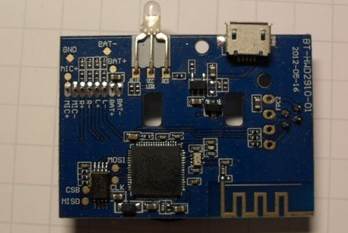
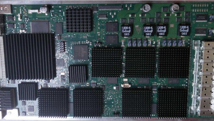
Precautions for the preservation of BGA in the SMT process
With the development of electronic technology, electronic components are developing in the direction of miniaturization and high-density integration. BGA components have been more and more widely used in SMT assembly technology, and with the emergence of u BGA and CSP, the difficulty of SMT assembly is becoming more and more difficult, and the process requirements are getting higher and higher. Due to the difficulty of repairing BGA, achieving good soldering of BGA is a topic for all SMT engineers. The following mainly introduces the precautions for the preservation and use of BGA.
Precautions for the preservation of BGA:
BGA components are highly temperature-sensitive components, so BGA must be stored under constant temperature and dry conditions. Operators should strictly abide by the operating process to prevent components from being affected before assembly. Generally speaking, the ideal storage environment for BGA is 200C-250C, and the humidity is less than 10%RH (nitrogen protection is better).
In most cases, we will notice the moisture-proof treatment of the BGA before opening the package of the component. At the same time, we should also pay attention to the time that the component package should not be exposed during the installation and soldering process to prevent The components are affected and the welding quality is reduced or the electrical performance of the components is changed.

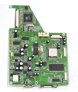
The difference between SMT patch technology and traditional through-hole insertion technology
The characteristics of SMT process technology can be compared with the traditional through-hole insertion technology (THT). From the perspective of assembly process technology, the fundamental difference between SMT and THT is "sticking" and "inserting." The difference between the two is also reflected in all aspects of the substrate, components, component shape, solder joint shape and assembly process method.
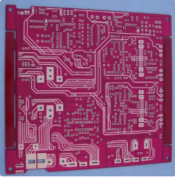
THT uses leaded components. The circuit connection wires and mounting holes are designed on the printed board. The component leads are inserted into the pre-drilled through holes on the PCB, and then temporarily fixed, wave soldering is used on the other side of the substrate. The brazing technology performs welding to form reliable solder joints and establish long-term mechanical and electrical connections. The main components and solder joints of the components are respectively distributed on both sides of the substrate. With this method, since the components have leads, when the circuit is dense to a certain extent, the problem of reducing the volume cannot be solved. At the same time, the faults caused by the proximity of the leads and the interference caused by the lead length are also difficult to eliminate.
The so-called SMT surface assembly technology refers to the chip structure components or the miniaturized components suitable for surface assembly, which are placed on the surface of the printed circuit board according to the requirements of the circuit, and assembled by soldering processes such as reflow soldering or wave soldering Together, it constitutes a certain function of electronic component patch processing and assembly technology.
The difference between SMT and THT component mounting and soldering methods: on the traditional THT printed circuit board, the components and solder joints are located on both sides of the board; while on the SMT circuit board, the solder joints and components are on the same board Surface. Therefore, on SMT printed circuit boards, through holes are only used to connect wires on both sides of the circuit board, the number of holes is much smaller, and the diameter of the holes is much smaller. In this way, the assembly density of the circuit board can be greatly improved.