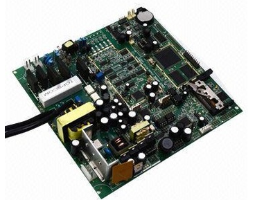
In the electronics industry, SMT chip processing is mainly processed by SMT, and many failures will occur during use. According to statistics, 60% of defects are caused by solder paste printing. Therefore, guaranteeing the high-quality printing quality of the SMT patch is an important prerequisite for guaranteeing its processing quality. Here's how to solve printing errors during the repair process.
1. There is no gap between the stencil and the PCB printing method, that is, "touch printing". High stability requirements for various structures, suitable for printing high-precision solder paste. The metal plate is in good contact with the printed board and can be separated from the PCB after printing. Therefore, this method has high printing accuracy and is especially suitable for fine and super macro printing.
1. Printing speed.
The solder paste rolls forward while scraping. Suitable for screen printing and fast printing.
This kind of rebound can also prevent the leakage of solder paste. Moreover, the slurry cannot be rolled in the net, resulting in clear solder paste, so the printing is too fast.
The dimension of is 10*20 mm/sec.
2. Printing method:

Contact or non-contact printing. The printing method for screen printing and printed circuit boards with blank spaces is "non-contact printing", generally 0.5*1.0mm, which is suitable for solder pastes of different viscosities. Push the solder paste into the steel mesh and press the PCB board with a scraper. After the scraper is removed, the steel mesh is isolated from the PCB board, thereby reducing the risk of vacuum leakage to the steel mesh.
3. Scraper type:
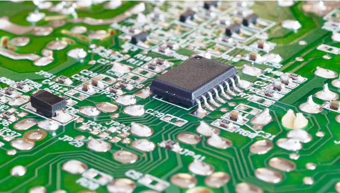
scrapers are divided into plastic scrapers and steel scrapers. For ICs whose distance is less than 0.5mm, steel solder paste can be used to form solder paste after printing.
4. Scraper adjustment.
During welding, the squeegee operating point is printed along the 45° direction, which can significantly improve the unevenness of the opening and reduce the damage of the thin steel plate with the opening. The pressure of the squeegee is usually 30N/mm.
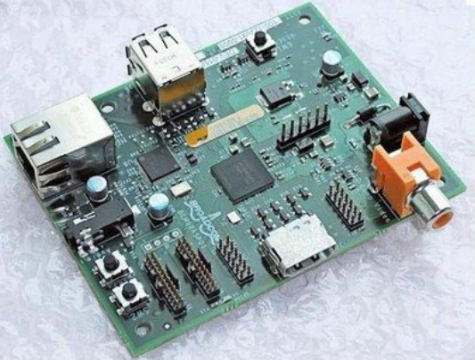
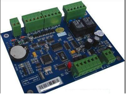
SMT chip processing
2. When installing, choose an IC mounting height with a pitch of no more than 0.5mm, 0mm or 0~-0.1mm mounting height to avoid solder paste falling off due to too low mounting height and short circuit during reflow.
Three, remelting welding.
The main reasons for assembly failure caused by reflow welding are as follows:
One, heating up too fast;
B. High temperature and overheating;
The heating speed of solder paste is faster than the heating speed of the circuit board;
D. Excessive amount of water.
Therefore, when determining the remelting welding process parameters, all factors should be fully considered to ensure that there is no problem with the welding quality before mass assembly.
SMT processing lead-free soldering and maintenance introduction
The introduction of lead-free SMT patch assembly has always been a challenge for the first assembly, because it will face more challenges when processing and rework are required. PCBA maintenance in a lead-free environment will have higher costs, quality details, time and repeatability issues-but due to lead-free requirements, these issues need attention. Due to the need for lead-free processes:
1. Train operators for lead-free assembly, maintenance and inspection, and evaluate time and cost.
2. Lead-free solder materials, etc. are all higher than traditional prices, such as lead-free wires, soldering rods, and core solders.
3. The processing temperature of lead-free assembly (about 30-35°C) requires higher precision and precision.
4. Lead-free technology also requires the research and planning of SMT processing plants to establish the correct PCBA repair process.
believes that the best practice of PCB assembly rework, first of all, it is necessary to profile the technical personnel according to the characteristics of the lead-free process. Define the rework standard, whether it requires standard solder or lead-free solder, the process is the same-the required steps are:
1. Define and execute accurate thermal profile.
2. The faulty component must be removed.
3. Clean up all rust or solder residues on site and prepare for new components.
4. Replace the parts with new solder and flux and reflow.
5. Rework is thoroughly inspected.
In a lead-free environment, accurate and reliable rework is more difficult, because PCBA and the components closest to maintenance must go through multiple high temperature cycles. In order to protect the stability of the circuit board, the preheating temperature should be set within the range not higher than the glass transition temperature of the PCB material.
The subsequent steps involved in the rework process vary depending on the lead-free requirements. The difference between standard and lead-free brings many challenges, which can only be solved by introducing new or changed technologies, including stricter and more accurate thermal curves and extremely high accuracy during the entire PCBA repair process. In this way, many expensive problems caused by different heat distribution can be avoided.