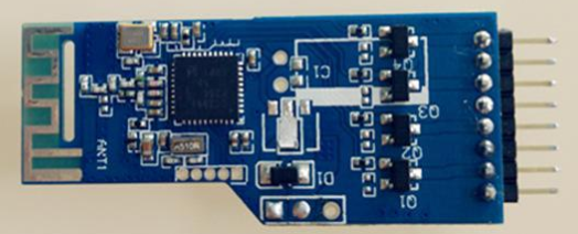
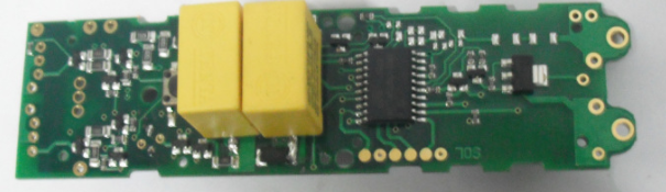
Placement programming operation on SMT placement machine
1. Edit the optimized product program on the SMT placement machine
1. Call up the optimized program.
2. Make the image of PCB MarK and partial Mak.
3. Make images for the components that are not imaged, and register them in the image library.
4. Register the unregistered components in the component library.
5. For multi-tube vibrating feeders with unreasonable emissions, redistribute them according to the length of the device body, and try to arrange the devices with a relatively close device body length on the same rack: hold the material station tightly, Try not to have an idle material station in the middle, so as to shorten the distance of picking up components.
6. Change the multi-pin, narrow-pitch devices with larger outlines in the program, such as QFPs with more than 160 pins, large-size PLCC, BGA, and long sockets, to Single Pickup, which can improve the placement. Installation accuracy.

7. Save to the disk to check whether there is any error message, and modify the program according to the error message until there is no error message after saving.
2. Proofreading check and backup patch program
1. According to the component list in the PCBA process file, check whether the component name, tag, model specification of each step in the program is correct, and correct the incorrect part according to the process file.
2. Check whether the components on each feeder station of the placement machine are consistent with the picking program table.
3. Use the main camera on the placement machine to check whether the X and Y coordinates of the components in each step are consistent with the component centers on the PCB. Check whether the corner Θ is correct according to the component position diagram in the process file, and correct the incorrect ones. (If you do not perform this step, you can correct it according to the actual placement deviation after the first SMT is placed)
4. Copy the completely correct product program to the backup U disk and save it.
6. Production can only be carried out after the proofreading and inspection are completely correct.
The main quality inspection process of smt patch processing products
In order to ensure the yield rate of PCBA foundry materials, the SMT factory must inspect the processed electronic products during the smt processing in Kunshan. The main quality inspection process problems of the products processed by the smt in Kunshan smt.
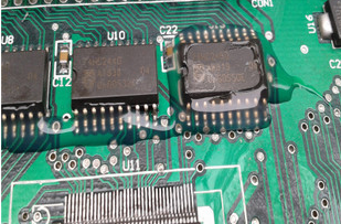
1. The surface of the FPC board should not affect the appearance of the solder paste, foreign matter and traces. The bonding position of the components processed by the smt patch should be free of rosin or flux and foreign objects that affect the appearance and soldering tin. There should be no wire drawing or tipping in the forming of the lower tin point of the component.
2. Component installation process. In the smt patch processing, the component placement position should be neat and centered, and there should be no offset or skewing; the type and specification of the components placed in the smt patch processing should be correct; the components processed by the smt patch processing cannot Lack of stickers or wrong stickers in the village; during smt patch processing, pay attention to components that cannot be reversed; during smt patch processing, the patch device with polarity requirements must be carried out in accordance with the polarity instructions.
3. The position of the tin paste in the printing process must not be significantly deviated in the middle, and the tin paste and soldering must not be affected. If the printing tin paste is moderate and can be well pasted, there is still no shortage of tin or too much tin paste. The tin paste is well formed, and there is no tin connection and unevenness.
4. Appearance of components There are no cracks and cuts on the bottom, surface, copper foil, wires, and through holes of the board. The FPC board is parallel to the plane and there is no deformation. The identification information characters processed by smt patch are unambiguous, offset printing, reverse printing, offset printing, double shadow, etc. The outer surface of the fpc board should not expand the bubble phenomenon. The aperture size meets the design requirements.