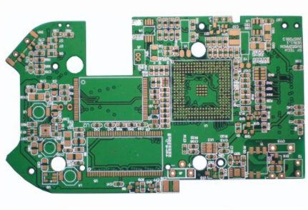
About SMT patch processing template production process requirements
1. What are the processing steps of Mark?
1. Mark processing method, whether Mark is needed, put it on the side of the template, etc.
2. On which side of the template the Mark graphic is placed, it should be determined according to the specific structure of the printing press (position of the camera).
3. Mark dot engraving method depends on the printing machine, including printing surface, non-printing surface, half engraving on both sides, full engraving and sealing vinyl, etc.
2. Whether to join the board, and the requirements of the board. If the board is assembled, the PCB file of the board should be given.
Third, the requirements of the insertion pad ring. Since the reflow soldering process is used for the plug-in components, a larger amount of solder paste is required than the mounting components, so if there are plug-in components that need to use the reflow soldering process, special requirements can be put forward.

Fourth, the modification requirements for the size and shape of the template (pad) opening. For pads that are usually larger than 3mm, in order to prevent the solder paste pattern from sinking and to prevent solder beading, the opening adopts a "bridging" method. The line width is 0.4mm, so that the opening is less than 3mm, which can be divided equally according to the size of the pad. Various components have requirements on template thickness and opening size.
1. The printing quality of μBGA/CSP and Flip Chip with square opening is better than that with circular opening.
2. When no-clean solder paste is used and no-clean process is used, the opening size of the template should be reduced by 5% to 10%:
3. The opening design of the lead-free process template is larger than that of lead, and the solder paste covers the pad as much as possible.
4. Appropriate opening shape can improve the processing effect of SMT patch. For example, when the chip component size is smaller than metric 1005, since the distance between the two pads is very small, the solder paste on the pads at both ends of the chip is easy to adhere to the bottom of the component, and it is easy to produce the bottom of the component after reflow soldering. Bridges and solder balls. Therefore, when processing the template, the inside of a pair of rectangular pad openings can be modified into a sharp or arcuate shape to reduce the amount of solder paste at the bottom of the component, which can improve the soldering sound adhesion at the bottom of the component during placement, as shown in the figure. The specific modification plan can be determined by referring to the "Printing Solder Paste Template Opening Design" of the template processing plant.
Five, other requirements
1. According to the PCB design requirements, whether the test point needs to be opened, etc., if there is no special description for the test point, it will not be opened.
2. Whether there are electro-polishing process requirements. The electropolishing process is used for templates with an opening center distance of less than 0.5mm.
3. Purpose (indicate whether the processed template is used for printing solder paste or printing patch glue).
4. Whether it is necessary to engrave characters on the template (you can engrave information such as PCB product code, template thickness, processing date, etc., but not through).
6. After receiving the Emil and the fax, the template processing factory will send back the fax of "please confirm by the buyer" according to the request of the buyer.
1. If you have any questions, call or fax it again, and you can process it after the buyer confirms it.
2. Check whether the size of the screen frame meets the requirements, place the template flat on the desktop, press the surface of the stainless steel screen with your hand, and check the tension.
Net quality, the tighter the stretch, the better the printing quality. In addition, the bonding quality around the screen frame should also be checked.
3. Lift the template and inspect it visually, check the appearance quality of the template opening, and check whether there are obvious defects, such as the shape of the opening and the distance between the adjacent openings of the IC pins.
4. Use a magnifying glass or microscope to check whether the bell mouth of the pad opening is down, whether the inner wall around the opening is smooth and whether there are burrs, and focus on the processing quality of the narrow-pitch IC pin opening.
5. Place the printed board of the product under the template, align the leak hole of the template with the printed board land pattern, check whether the pattern is completely aligned, whether there are holes (unnecessary openings) and few holes (floor drain Opening).
6. If a problem is found, first check whether it belongs to our confirmation error, and then check whether it is a processing problem. If a quality problem is found, it should be reported to the template PCB manufacturing and processing plant and negotiated to resolve it.