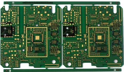
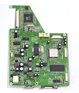
Up to now, there are still many PCB circuit boards still undergoing the wave soldering process, thinking that the wave furnace has already been put into the museum! However, most of what is going now is the selective wave soldering (Selective Wave Soldering) process, rather than the earlier process of soaking the entire panel in a tin furnace.
Wave soldering
The so-called selective wave soldering still uses the original tin furnace, the difference is that the board needs to be placed in the tin furnace carrier/tray (carrier), and then the parts that need wave soldering are exposed and tinned, other parts It is covered with a carrier to protect it, which is a bit like putting a lifebuoy in a swimming pool. The place covered by the lifebuoy will not get water. If it is replaced with a tin stove, the place covered by the carrier will naturally not If it is stained with tin, there will be no problem of remelting tin or dropping parts.
But not all boards can use the selective wave soldering (Selective Wave Soldering) process. If you want to use it, there are still some design restrictions. The most important condition is that these parts selected for wave soldering must be compatible with other parts. The parts that do not need wave soldering have a certain distance, so that the solder furnace carrier can be made.
Precautions for selective wave soldering carrier and circuit design:
When the solder pins of the traditional plug-in are too close to the edge of the carrier, the problem of solder insufficiency is likely to occur due to the shadow effect.

The carrier must cover the parts that do not need to be soldered with a tin furnace.
It is recommended to keep at least 0.05” (1.27mm) of the wall thickness on the edge of the hole of the carrier to prevent penetration of the solder into the parts that do not need to be soldered with a tin furnace.
It is recommended to keep at least 0.1” (2.54mm) away from the edge of the hole of the carrier for parts that need to be soldered by a tin furnace to reduce the possible shadow effect.
The height of the parts passing the furnace surface should be less than 0.15” (3.8mm), otherwise the furnace carrier will not be able to cover these high parts.
The material of the soldering furnace carrier must not react with the solder, and it must be able to withstand repeated high heat cycles without deformation, not easy to absorb heat, and be as light as possible, with less heat shrinkage. At present, there are more people. The material used is aluminum alloy, and there are also synthetic stone materials.
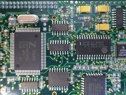
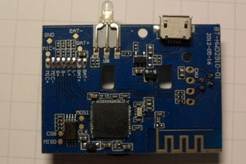
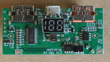
In fact, when the circuit boards first came out, they were almost always designed with traditional INSERTION operations. All the boards needed to go through wave soldering. At that time, the boards were only single-sided; after the invention of SMT, The mixed use of SMT and wave soldering began to appear, because at that time there was still a large part of the parts that could not be converted to the SMT process, that is to say, there are still many traditional plug-in parts, so all the parts must be put into the design of the board. The plug-in parts are arranged on the same side, and then the other side is used for wave soldering. The SMT parts on the wave soldering side must be fixed with red glue to prevent the parts from falling into the soldering furnace when passing through the wave soldering furnace. Now almost all boards have adopted the SMT process on both sides, but it seems that there are still very few parts that cannot be replaced by the SMT process, so this selective wave soldering process came into being.