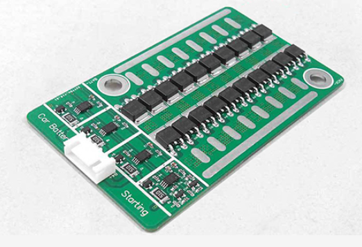
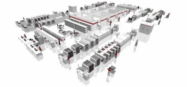
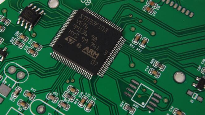
I believe that all friends who have done SMT chip processing know that PCBA boards must be reflow soldered after the devices are mounted on the placement machine. However, board bending and board warping are prone to occur during PCBA reflow soldering, so how to prevent the circuit board from going through the reflow furnace from board warping and board warping, then I will introduce the relevant countermeasures.
1. Reduce the influence of temperature on the stress of the circuit board
Since "temperature" is the main source of circuit board stress, as long as the temperature of the reflow furnace is reduced or the rate of heating and cooling of the circuit board production in the reflow furnace is slowed, the bending and warpage of the board can be greatly reduced. happen. However, other side effects may occur, such as solder short circuit.

2. PCB with high Tg board
Tg is the glass transition temperature, that is, the temperature at which the material changes from the glass state to the rubber state. The lower the Tg value of the material, the faster the circuit board starts to soften after entering the reflow furnace, and it becomes soft rubber state The time will also be longer, and the deformation of the circuit board will of course be more serious. Using a higher Tg board can increase its ability to withstand stress and deformation, but the price of high TgPCB board is relatively higher.
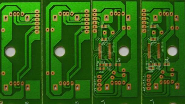
3. Increase the thickness of the circuit board
In order to achieve the purpose of lighter and thinner for many electronic products, the thickness of the circuit board has left 1.0mm, 0.8mm, or even 0.6mm. Such a thickness must keep the circuit board from deforming after the reflow furnace, which is really a bit It is difficult for others. It is recommended that if there is no requirement for lightness and thinness, the thickness of the circuit board is preferably 1.6mm, which can greatly reduce the risk of bending and deformation of the board.
4. Reduce the size of the circuit board and reduce the number of puzzles
Since most of the reflow furnaces use chains to drive the circuit board forward, the larger the PCB design size, the circuit board will dent and deform in the reflow furnace due to its own weight, so try to treat the long side of the circuit board as the edge of the board. Putting it on the chain of the reflow furnace can reduce the depression and deformation caused by the weight of the circuit board itself. The reduction in the number of panels is also based on this reason. Reach the lowest amount of depression deformation.
5. Used furnace tray fixture
If the above methods are difficult to achieve, the last is to use the furnace tray to reduce the amount of deformation. The furnace tray can reduce the bending and warpage of the board because whether it is thermal expansion or cold contraction, it is hoped that the tray can fix the circuit board. After the temperature of the circuit board is lower than the Tg value and starts to harden again, the original size can be maintained.
If the single-layer pallet cannot reduce the deformation of the PCB circuit board, another layer of cover must be added to clamp the circuit board with the upper and lower pallets, which can greatly reduce the problem of circuit board deformation through the reflow furnace. However, this furnace tray is quite expensive, and manual labor is required to place and recycle the trays.