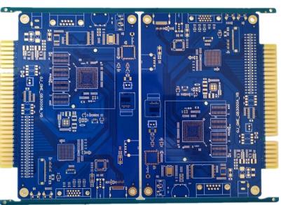
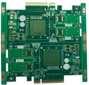
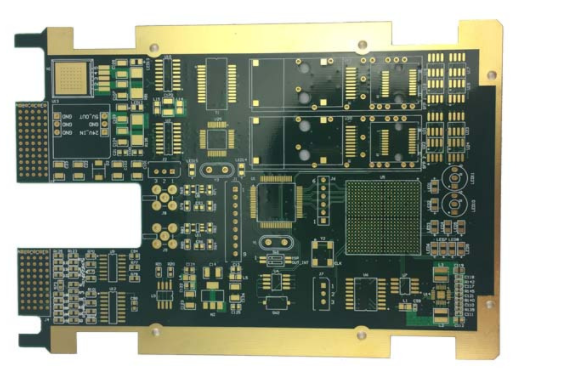
How large is the design line width and line spacing rules of multilayer circuit boards?
For many new entrants, it is not clear what the line width of the multilayer circuit board should be set to. The editor of Shenzhen Factory will explain here.
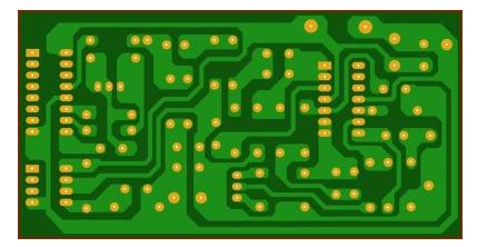
For the setting of the wiring width of the multilayer circuit board, there are mainly two issues to be considered:
One is the amount of current flowing. For example, for power lines, the current flowing through the circuit needs to be considered. If the current flowing through is large, the wiring should not be too thin.
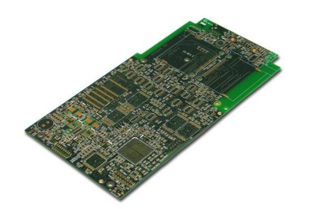
Actual measurement: current carrying capacity of multilayer circuit board traces and vias
The second is to consider the actual board manufacturing capacity of the multilayer circuit board factory. If the required current is very small (such as a signal line), it can be made thinner. Sometimes the PCB circuit board area is small and there are many components, and you want to make the wiring as thin as possible, but if it is too thin, the circuit board factory may not be able to make it, or it can not be made but the defect rate increases. This can be confirmed with the multilayer circuit board factory. As far as I know, the line width is 0.2mm and the line spacing is 0.2mm, which can be done by ordinary circuit board manufacturers. The line width of 0.127mm is not always possible. The industry's minimum line width standard should be 0.1mm. The follow-up may be more detailed with the development of technology.

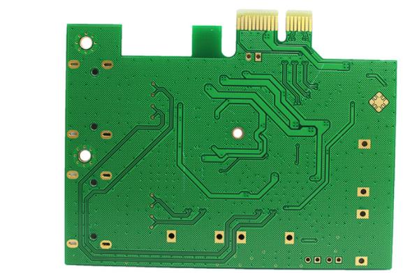
As for the size of the vias, you can also directly confirm with the circuit board factory. After all, even if you use small-aperture vias to design a PCB multi-layer circuit board, there are many multi-layer circuit board manufacturers that can’t do it, or can do it but the cost is high. no. As far as I know, the outer diameter is 0.5mm and the inner diameter is 0.3mm. Basically all board manufacturers can do it.
1. PCB multilayer circuit boards need to be impedance signal lines, which should be set in strict accordance with the line width and line spacing calculated by the stack. For example, radio frequency signals (conventional 50R control), important single-ended 50R, differential 90R, differential 100R and other signal lines, the specific line width and line spacing can be calculated by stacking.
2. The designed line width and line spacing should consider the production process capability of the selected multilayer circuit board factory. If the line width and line spacing are set to exceed the process capability of the cooperative circuit board manufacturer during the design, unnecessary production costs need to be added., But the design can not be produced. Generally, the line width and line spacing are controlled to 6/6mil under normal circumstances, and the via hole is 12mil (0.3mm). Basically, more than 80% of the circuit board manufacturers can produce it, and the production cost is the lowest. The minimum line width and line spacing is controlled to 4/4mil, and the via hole is 8mil (0.2mm). Basically, more than 70% of the circuit board manufacturers can produce it, but the price is slightly more expensive than the first case, not too expensive. The minimum line width and line spacing is controlled to 3.5/3.5mil, and the via hole is 8mil (0.2mm). At this time, some circuit board manufacturers cannot produce it, and the price will be more expensive. The minimum line width and line spacing is controlled to 2/2mil, and the via hole is 4mil (0.1mm, at this time, it is generally HDI blind buried via design, and laser vias are required). At this time, most circuit board manufacturers cannot produce it, and the price is the most Dear. The line width and line spacing here refer to the size between elements such as line-to-hole, line-to-line, line-to-pad, line-to-via, and hole-to-disk when setting rules.
3. Set rules to consider the design bottleneck in the design file. If there is a 1mm BGA chip, the pin depth is relatively shallow, only one signal line is needed between the two rows of pins, which can be set to 6/6 mil, the pin depth is deeper, and two rows of pins are required The signal line is set to 4/4mil; there is a 0.65mm BGA chip, generally set to 4/4mil; there is a 0.5mm BGA chip, the general line width and line spacing must be set to 3.5/3.5mil; there is a 0.4mm BGA Chips generally require HDI design. Generally, for the design bottleneck, you can set regional rules (see the end of the article for the setting method), set the local line width and line spacing to be smaller, and set the rules for other parts of the PCB to be larger, so as to facilitate production and improve the qualified rate of PCBs.
4. It needs to be set according to the density of the multilayer circuit board design. The density is smaller and the board is looser. The line width and line spacing can be set to be larger, and vice versa. The routine can be set according to the following steps:
1. 8/8mil, 12mil (0.3mm) for via hole.
2. 6/6mil, 12mil (0.3mm) for via hole.
3. 4/4mil, 8mil (0.2mm) for via hole.
4. 3.5/3.5mil, 8mil (0.2mm) for via hole.
5. 3.5/3.5mil, 4mil (0.1mm, laser drilling) for via hole.
6. 2/2mil, 4mil (0.1mm, laser drilling) for via hole.