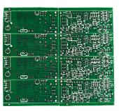
There are many types o fPCB circuit boards, including single-sided PCB circuit boards, double-sided PCB circuit boards, etc. Regarding PCB circuit boards, there are too many professional terms designed, and people in the general industry can only explain single-sided PCB circuit boards clearly.
1. The Voltage Plane voltage layer should have been heard by everyone. In fact, it refers to the voltage required to drive various parts on a single-sided PCB circuit board, which can be supplied by a common copper conductor area on the board, or a multilayer board One level is used as the voltage layer. For example, one of the two inner layers of a four-layer board is the voltage layer (such as 5V or 12V), which is generally represented by the Vcc symbol. The other layer is the ground plane (Groung Plane). Generally, the voltage layer of the multi-layer board not only supplies the voltage required by the parts, but also doubles the function of heat sinking and shielding;

2. Voltage Plane Clearance is actually the empty ring of the voltage layer. When the plated through holes must pass through the built-in voltage layer of the multilayer board and do not want to contact with it, they can be etched on the copper surface of the voltage layer first. After pressing the circular open space, drill a smaller hole in this slightly larger open space, and continue to complete the PTH. At this time, between the copper wall of the tubular hole and the large copper surface of the voltage layer, there is an empty ring that can be insulated, which is called Clearance;
3. Thermo-Via thermal hole, this should not be unfamiliar. It refers to high-power parts such as large ICs on single-sided PCB circui t boards. A large amount of heat will be generated during work. The assembly board must dissipate this extra heat., So as not to damage the life of the electronic equipment. One of the simple ways to dissipate heat is to make use of the open space of the base plate of the large IC on the surface, deliberately add PTH, and direct the heat from the large IC to the large copper surface on the back of the board for heat dissipation. This kind of through hole dedicated to heat transfer but not conductive is called Thermo-Via;
4. Thermal Relief refers to the heat-dissipating hollow. Regardless of the large copper surface on the inner and outer layers, the continuous and complete area must not be too large, so as to prevent the board from being in high temperature (such as welding), due to the gap between the plate and the copper The difference in expansion coefficient causes problems such as warping, floating, or blistering. Generally, a "tennis racket" type hollowing can be used on the large copper surface to reduce thermal shock. This term is also called Halfonning or Crosshatching. UL stipulates that in its certified "yellow card", the diameter of the largest copper surface that needs to be printed on the board is a safety consideration.
The terminology of single-sided PCB circuit boards is easier to understand, and science popularization is the purpose!