In the process of PCB manufacturing, there will be many unexpected situations, such as electroplating copper, electroless copper plating, gold plating, tin-lead alloy plating and other plating layer delamination. So what is the reason for this kind of stratification? Next, iPCB board factory ipb will analyze the reasons for the delamination of PCB plating.
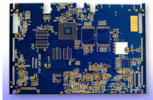
PCB board
Analysis on the Causes of PCB Electroplating Delamination
Under ultraviolet light irradiation, the photoinitiator that has absorbed the light energy decomposes into free radicals to initiate a photopolymerization reaction, forming a body-shaped molecule that is insoluble in a dilute alkali solution. When the exposure is insufficient, due to incomplete polymerization, the film swells and becomes soft during the development process, resulting in unclear lines or even the film layer falling off, resulting in poor bonding between the film and copper; if the exposure is overexposed, it will cause development difficulties and also during the electroplating process. Warping and peeling occurred during the process, forming penetration plating.
Therefore, it is important to control the exposure energy; after the copper surface is treated, the cleaning time is not easy to be too long, because the cleaning water also contains a certain acidic substance. Although its content is weak, the impact on the copper surface should not be taken lightly. It should be strictly in accordance with the PCB system. The cleaning operation shall be carried out at the time specified in the board process specification.
The main reason why the gold layer falls off the surface of the nickel layer is the surface treatment of the nickel. The poor surface activity of nickel metal is difficult to achieve satisfactory results. The surface of the nickel plating layer is prone to produce a passivation film in the air. If improperly handled, the gold layer will be separated from the surface of the nickel layer. If improper activation is performed during gold electroplating, the gold layer will peel off from the surface of the nickel layer. The second reason is that after activation, the cleaning time is too long, causing a passivation film on the nickel surface to regenerate, and then gold plating will inevitably cause the defect of the plating layer to fall off.
There are actually many reasons for PCB electroplating delamination. If you want to avoid similar situations in the process of PCB manufacturing, it is of great concern to the care and responsibility of the technicians. Therefore, an excellent PCB manufacturer will conduct high-standard training for every workshop employee in order to prevent inferior products from leaving the factory.

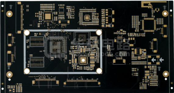
PCB board factory
iPCB manufacturing capability
The energy production is from 2 to 14 layers, and the 14-22 layers can be sampled and produced.
Minimum line width/spacing: 3mil/3milBGA spacing: 0.20MM
The smallest aperture of the finished product: 0.1mm Size: 610mmX1200mm
Ink: Tamura, Taiyo, Fudokken from Japan;
FR4: Shengyi, Kingboard, Haigang, Hongren, Guoji, Hazheng, Nanya,
(Shengyi S1130/S1141/S1170), Tg130 degree Celsius/ Tg170 degree Celsius Tg180 degree Celsius Contour TG sheet)
High frequency board: Rogers (Rogers), Taconic, ARLLON;
Surface technology: tin spray, lead-free tin spray, immersion gold, full board gold plating, plug gold plating, full board thick gold, chemical tin (silver), anti-oxidation (OSP) blue glue, carbon oil.