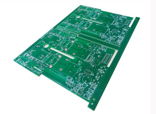
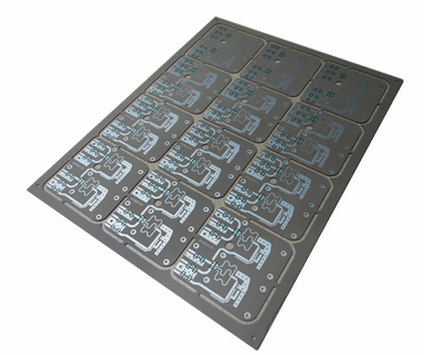
At present, in the field of electronic product processing, multilayer circuit boards are indispensable as one of the important electronic components. At present, there are many types of PCB circuit boards, such as high-frequency circuit board plates, microwave circuit boards and other types of printed circuit boards that have gained a certain reputation in the market. Multilayer circuit board factories have specific processing techniques for various board types. But in general, multilayer circuit board manufacturers need to consider three major aspects:
1. Consider the choice of process flow
The production of multi-layer circuit boards is prone to be affected by many factors, and the number of processing layers, punching technology, surface coating treatment and other technological processes will all affect the quality of the finished PCB circuit board. Therefore, for these process environments, multilayer circuit board production is fully considered in combination with the characteristics of the production equipment, and can be flexibly adjusted according to the types of PCB boards and processing requirements.
2. Consider the choice of substrate
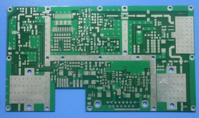
The substrates of circuit boards can be divided into two categories: organic materials and inorganic materials. Each material has its own unique advantages. Therefore, the determination of the type of substrate considers various properties such as dielectric properties, copper foil type, base groove thickness, and processability characteristics. Among them, the thickness of the surface copper foil is a key factor affecting the performance of this printed circuit board. Generally speaking, the thinner the thickness, the more convenient the etching and the improvement of the precision of the graphics.

3. Consider the setting of the production environment
The environment of the multi-layer circuit board manufacturing workshop is also a very important aspect, and the regulation of ambient temperature and ambient humidity are both crucial factors. If the ambient temperature changes too significantly, it may cause the holes on the base plate to break. If the environmental humidity is too high, nuclear energy will have an adverse effect on the performance of the substrate with strong water absorption, specifically in terms of dielectric properties. Therefore, it is very necessary for circuit board manufacturers to maintain proper environmental conditions during production.
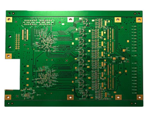
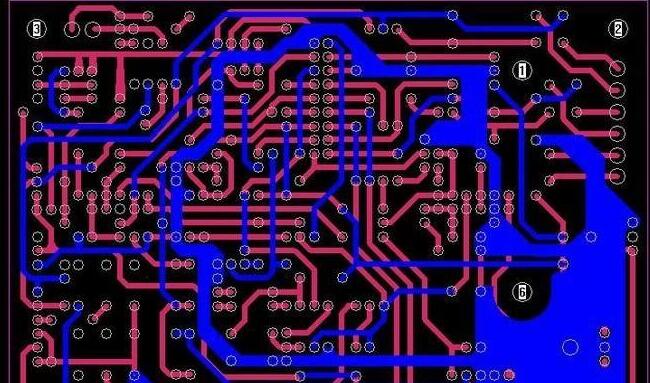
Multi-layer blind buried, blind hole structure printed circuit boar ds are generally completed by "sub-board" production methods, which means that they must be completed through multiple pressing, drilling, and hole plating, so precise positioning is very important.
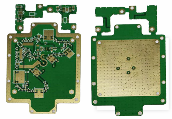
The high-precision printed circuit refers to the use of fine line width/spacing, micro holes, narrow ring width (or no ring width), and buried and blind holes to achieve high density. High precision means that the result of "fine, small, narrow, and thin" will inevitably lead to high precision requirements. Take the line width as an example: O.20mm line width, if it is produced in accordance with the regulations, it is qualified to produce 0.16-0.24mm. The error is (O.20 soil 0.04) mm; and the line width of O.10 mm, the error is (0.10 ± O.02) mm, obviously the accuracy of the latter is doubled, and so on is not difficult to understand, Therefore, the high-precision requirements will not be discussed separately.
Buried, blind, and through-hole (multi-layer blind-buried circuit boards) combined technology is also an important way to increase the density of printed circuits. Generally, the buried and blind holes are tiny holes. In addition to increasing the number of wiring on the circuit board, the buried and blind holes are interconnected by the "nearest" inner layer, which greatly reduces the number of through holes formed, and the isolation disk is also set up. It will be greatly reduced, thereby increasing the number of effective wiring and inter-layer interconnections in the board, and increasing the density of interconnections.
The Problem of Coincidence Between Layers in the Manufacturing of Blind and Buried Multilayer Circuit Boards
By adopting the pin front positioning system of ordinary multi-layer circuit board production, the graphic production of each layer of single chip is unified into a positioning system, which creates conditions for the realization of successful manufacturing. For the ultra-thick single chip used this time, if the board thickness reaches 2 mm, a certain thickness layer can be milled at the location of the positioning hole, and it is also attributed to the processing of the four-slot positioning hole punching equipment of the front positioning system Ability.