How do PCB factory's circuit boards make? PCB factory's circuit board itself is made of insulating and heat-insulating materials that are not easy to bend. The small circuit material that can be seen on the surface is copper foil. The copper foil was originally covered on the entire PCB board, but part of it was etched away during the manufacturing process, and the remaining part became a network of small circuits NS.
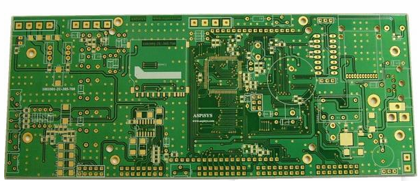
These lines are called wires or wiring, and are used to provide circuit connections for parts on the PCB. Usually the color of PCB board is green or brown, which is the color of solder mask. It is an insulating protective layer that can protect the copper wire and prevent parts from being welded to the wrong place.
Multilayer boards are now used on motherboards and graphics cards, greatly increasing the area that can be wired. Multilayer boards use more single or double-sided wiring boards, and put a layer of insulating layer between each layer of boards and press them together. The number of layers of the PCB board means that there are several independent wiring layers. Usually the number of layers is an even number and contains the two outermost layers. Common PCB boards generally have a structure of 4 to 8 layers. The number of layers of many PCB boards can be seen by looking at the cut surface of the PCB board. But in fact, no one can have such good eyesight. So, let me teach you one more method below.
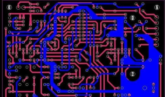
The circuit connection of the multilayer board is through buried via and blind via technology. Most motherboards and display cards use 4-layer PCB boards, and some use 6, 8-layer, or even 10-layer PCB boards. If you want to see how many layers the PCB has, you can identify it by observing the via holes, because the 4-layer boards used on the motherboard and display card are traces on the first and fourth layers, and the other layers have other uses (ground wires). And power supply).
Therefore, like the double-layer board, the via hole will penetrate the PCB board. If some guide holes appear on the front side of the PCB board but cannot be found on the back side, then it must be a 6/8-layer board. If the same via holes can be found on both sides of the PCB board, it will naturally be a 4-layer board.

The PCB manufacturing process begins with a PCB "substrate" made of glass epoxy (Glass Epoxy) or similar materials. The first step of production is to lightly draw the wiring between the parts. The method is to "print" the circuit negative of the designed PCB circuit board on the metal conductor by using a negative transfer (Subtractive transfer) method.
This technique is to spread a thin layer of copper foil on the entire surface and eliminate the excess. And if you are making a double-sided board, then both sides of the PCB substrate will be covered with copper foil. To make a multi-layer board, the two double-sided boards can be "pressed" together with a special adhesive.
Next, the drilling and electroplating required to connect the components can be performed on the PCB board. After drilling by the machine according to the drilling requirements, the inside of the hole must be electroplated (Plated-Through-Hole technology, PTH). After the inside of Kongbi is metal treated, the inner layers of the circuit can be connected to each other.
Before starting electroplating, the debris in the hole must be cleaned. This is because the resin epoxy will produce some chemical changes after heating, and it will cover the internal PCB layer, so it must be removed first. Both cleaning and electroplating actions are completed in the chemical process. Next, the solder mask (solder mask ink) needs to be covered on the outermost wiring, so that the wiring will not touch the electroplated part.
Then, the various components are printed on the circuit board to mark the position of the parts. It cannot cover any wiring or gold fingers, otherwise it may reduce the solderability or the stability of the current connection. In addition, if there is a metal connection part, the "golden finger" part is usually plated with gold at this time, so that high-quality current connection can be ensured when the expansion slot is inserted.
Finally, it's the test. To test whether the PCB has a short circuit or open circuit, you can use optical or electronic testing. The optical method uses scanning to find defects in each layer, and the electronic test usually uses a flying-probe to check all connections. Electronic testing is more accurate in finding short circuits or open circuits, but optical testing can more easily detect incorrect gaps between conductors.
After the circuit board substrate is completed, a finished motherboard is equipped with various large and small components on the PCB substrate according to the needs-first use the SMT automatic placement machine to "sold on the IC chip and chip components, and then manually connect it. Plug in some work that the machine can't do, and firmly fix these plug-in components on the PCB through the wave/reflow soldering process, so a motherboard is produced.