How to improve PCB pattern plating film
1. Preface: With the rapid development of the multilayer circuit board industry, PCBs are gradually turning to high-precision, small-aperture, and high-format reports. Copper holes need 20 to 25 microns, and the spacing of the DF lines is less than 4 meters.
Generally speaking, printed circuit systems deal with problems through electroplating. The sleeve will produce a direct short circuit, which will affect the one-time efficiency of the printed circuit board during the AOI inspection. A serious or too much coating cannot be directly repaired and brought directly to the scrap iron.
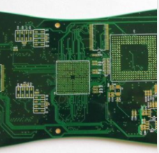
2. Graphical explanation of the problem of electroplating clamp: Principle analysis of PCB clamping
(1) The copper thickness of the pattern plating line is greater than the thickness of the dry film, which will result in a clamping film. (The thickness of the dry film used in the PCB plant is 1.4 MHz)
(2) The thickness of copper and tin in the photographic plating line may exceed the thickness of the dry film.
Third, the analysis of the reasons for the clamping of the PCB board
Easy to fasten the images and photos of the board. The lines are dense and the length/width are different. The minimum D/F is 2.8 meters (0.070 mm), the minimum hole is 0.25 mm, the thickness of the board is 2.0 mm, the format report is 8:1, and the copper requirement for the hole is greater than 20 m. This is the difficult part of the procedure.

2. Analysis of the reasons for clamping The current density of pattern plating is high, and the copper plating layer is too thick.
(2) There is no border at both ends of Feiba, and a thick film is electroplated in a highly dense area.
(3) The water shortage current of the buffalo is greater than the adjustment current of the actual production card. There are 2.5-3.5 ml of Atlant film too small. This is an uneven current, and the copper plating cylinder has not cleared the anode.
(Form) Bad When the equipment fails, the protection current of the circuit board in the copper cylinder is too long. The configuration mode of the project is unreasonable, and there is an error in the effective plating area provided by the project. The space between PCB cards is too small, and very difficult map circuit boards are easily clamped.
Four effective coating modes
1. Reduce the current density and appropriately extend the copper plating time.
2. Reduce the thickness of copper plating, reduce the density of copper plating, and reduce the thickness of copper plating.
3. The thickness of the copper plate is increased from 0.5oz to 1/3oz, so that the thickness of the copper plating layer is about 10 microns, which can reduce the current density and thickness of the copper plating.
4. Buy a dry film from 1.1.8 to 2.0 cubic meters of cardboard and use it for the test with an interval of less than 4 meters.
5. Other modes, such as composition, modification and compensation, line offset space, hole cutting ring and protective bag, can also relatively reduce the generation of pliers.
6. Control method for electroplating of lightly clamped plate
1. First, try the copper thickness, line width/interval and qualified impedance in the direction of the two steering wheels, and mark the map of the bus into the movement through inspection. If blocking is detected, immediately adjust the current to retest.
2. Fading of the film: For boards with a deviation of less than 4 meters, the fading rate of the film is an appropriate slow-down rate.
3. Skills of the staff of the present invention: When you use a simple clamping method to display the output current of the license plate, pay attention to the evaluation of the current density. Generally, when the minimum area of the board is less than 3.5 milliliters (0.088 mm), when the current density of copper electroplating is lower than 12 Asf, it is not easy to produce clamping.
4. Except for particularly difficult charts, the table is as follows: The lowest D/F space is 2.5 mm (0.063 mm), and it is difficult to get rid of the fate of sandwiches when the assembly line is well uniform. It is recommended that the D/F current density used to test FA is less than 10 Foss.
The minimum D/F space is 2.5 meters (0.0063 mm). There are many independent lines with inconsistent distribution. In general, the electroplating lines of PCB manufacturers have greater unity, and it is difficult to avoid the fate of sandwiches.
The printed copper plating used a current density of 14.5 AF * 65 minutes to make a sandwich. It is recommended that the current density of pattern plating is less than 11 Asf for testing FA. 6. Personal experience and summary For many years, I have been committed to dealing with the problem of PCBs. Fundamentally, every printed circuit board will have film clamping and low line spacing on the manufacturing board. The difference is that every factory has different films. Some companies have little perception of movies, while others have more movie claims.
2. Analyze the following factors:
1. Each company has different types of PCB structures, and PCB manufacturing processes are different.
2. Every enterprise has different management methods and methods.
3. Based on the experience I have accumulated for many years, we should first ensure the use of low-density current and extend the appropriate copper plating time to the low-space board.
The current indicator should be used to evaluate the current density and copper plating time based on experience, paying attention to the fuse mode and operation method. For plates whose minimum spacing is less than 4 mm, marchers in the test flight must successfully determine whether there is one or any of them.
It plays a role in quality control and prevention, so the probability of making a large series of movies is very low. I personally believe that good PCB quality requires not only experience and skills, but also good methods. It also depends on the performance of the production staff.
The pattern coating is different from the entire plate coating. The main difference lies in the need to plate circuit patterns on different types of maps.
Some circuit patterns are unevenly distributed. In addition to the width and spacing of the rows, there are multiple scattered lines, multiple isolation lines, and different independent hole patterns. Therefore, the author prefers to use FA (current) skills to solve or prevent the thick fur problem.
The scope of improvement action is small and rapid, and the preventive effect is obvious.