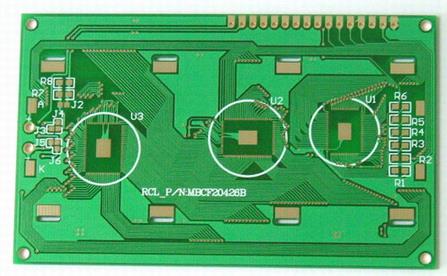
Basic rules of PCB layout
PCB manufacturers: First of all, the basic rules of component layout
1. According to the layout of circuit modules, related circuits that achieve the same function are called modules. Each part of the circuit module adopts the principle of near-field concentration, and the digital circuit is separated from the analog circuit.
2. Components and equipment must not be installed in non-installation holes (such as positioning holes and standard holes) of 1.27mm. Parts and components must not be installed around 3.5mm (M2.5) and 4mm (M3) mounting holes (such as screws).
one. Avoid placing holes under components such as horizontal resistors, inductors (plug-ins), electrolytic capacitors, etc., and avoid short circuits between the holes and the component shell after wave soldering.
4. The distance between the outer edge of the part and the edge of the board is 5 mm.
5. The distance between the outside of the pad of the mounted component and the outside of the adjacent mounted component is greater than 2 mm.
6. Metal shell parts and metal parts (shielding boxes, etc.) must not be in contact with other parts, and must not be tightly adhered to printed circuits and gaskets, and the spacing should be greater than 2mm. The square holes such as plate positioning holes, fastener installation holes, and elliptical holes are more than 3mm away from the edge of the plate.
7. The heating element shall not be adjacent to the conductor and the heating element, and the high temperature elements shall be evenly distributed.
8. The power socket should be as close as possible to the PCB board, and the bus connectors connected to the power socket should be set on the same side. Special care should be taken not to place power sockets and other welding connectors between the connectors in order to facilitate the welding of these sockets, connectors and power cord design and wiring. The distance between the power socket and the welding connector should be considered to facilitate the insertion and removal of the power plug.

9. Arrangement of other components:
All IC components are aligned on one side. The polarity of the polar component is obvious. The polarity of the same printed circuit board must not exceed two directions. When two directions appear, they are perpendicular to each other.
10. Surface wiring should be tight and appropriate. When the density difference is too large, the mesh should be filled with mesh copper foil, which should be larger than 8mm (or 0.2mm).
11. There should be no through holes on the patch gasket to avoid sticking loss and virtual soldering of components. Important signal wires are not allowed to pass through the socket pins.
12. One side of the patch is aligned, the direction of the characters and the direction of the encapsulation are the same.
13. The marking directions of polarized devices should be as consistent as possible.
two. Assembly wiring rules
1. It is not allowed to route wiring less than 1mm from the edge of the PCB board and 1mm around the mounting hole.
2. The power cord should be as wide as possible, no less than 18 miles; the width of the signal line should not be less than 12 mils; the CPU input and output lines should not be less than 10 mils (or 8 mils); the line spacing should not be less than 10 mils ;
three. Normal perforation shall not be less than 30 mills.
4. Dual in-line: 60 mil pad, 40 mil aperture;
1/4w resistance: 51*55mil (0805 label), directly inserted into 62mil pad and 42mil hole;
Non-polar capacitor: 51*55 mils (label 0805); 50 mils soldering pad, 28 mils aperture when directly inserted;
5. Try to pay attention to the radiation of the power line and the ground line, and the signal line has no loop.
ipcb is a high-precision, high-quality PCB manufacturer, such as: isola 370hr PCB, high-frequency PCB, high-speed PCB, ic substrate, ic test board, impedance PCB, HDI PCB, Rigid-Flex PCB, buried blind PCB, advanced PCB, microwave PCB, telfon PCB and other ipcb are good at PCB manufacturing.