Abstract: The pad design technology is the key to surface mount technology (smt). The key technologies in the pad pattern design are analyzed in detail, including the principle of component selection, rectangular passive components, SOIC and PLCC and QFP device pad optimization design. Afterwards, the problems related to pads when designing printed circuit boards are proposed.

1 Introduction
Surface mount technology (smt) is a complex system engineering, and smt design technology is the bridge and key technology between various smt support technologies. The smt design technology consists of four parts: smt circuit design, process design, equipment operation design and inspection design.
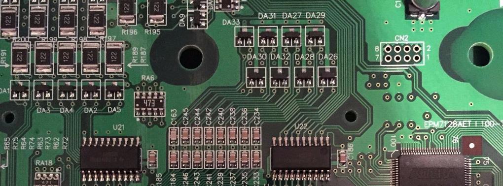
The smt pad graphic design is a key part of the printed circuit board design, (Nanjing smt) because it determines the welding position of the components on the printed circuit board, and the reliability of the solder joints and the welding that may occur during the welding process Defects, cleanability, testability, and overhaul volume all have a great impact. In other words, the design of the land pattern is one of the key factors that determine the manufacturability of surface mount components.
At present, there are many types and specifications of surface mount components SMC/SMD, different structures, and many manufacturers. Components that achieve the same function may have a variety of packaging forms; and for a given packaging type, there are also certain differences in its specifications and dimensions. Therefore, the establishment of a unified design specification is of great benefit to reducing the complexity of land pattern design and improving the reliability of solder joints.
The design of surface mount land patterns is closely related to two factors, component selection and process methods. Because a reasonable land pattern must match the component size, it can be used for slightly different components from different manufacturers, can adapt to various processes (such as reflow soldering and wave soldering), and meet the requirements of layout and wiring to a large extent.
2 Key technology in pad pattern design
2.1 The principle of selecting components
When selecting components, according to the requirements of the system and circuit principles and assembly process, and on the basis of ensuring that the functions and performance of the components are met, a limited number of suppliers are designated to provide suitable components to reduce the need for land pattern design. Tolerance, reduce the complexity of the land pattern design.
2.2 Rectangular passive component land pattern design
Passive components can be soldered by wave soldering, reflow soldering or other processes. As there are certain differences in the process and heat distribution of various soldering methods, from the perspective of optimizing the land pattern, different processes have different sizes of land patterns, because the components are prone to move and stand upright during the soldering process. (Nanjing smt) In the process of wave soldering, because the components are pasted with adhesive, the problem of component movement is not prominent. The good land pattern designed for reflow soldering is also suitable for wave soldering. The typical rectangular passive component land pattern is rectangular, as shown in Figure 1.
Figure 1 Typical rectangular passive component land pattern
The formula for calculating the pad size is:
A=Wmax-K (1)
When mounting capacitors: B=Hmax+Tmin-K (2)
When mounting resistors: B=Hmax+Tmin+K (3)
G=Lmax-2Tmax-K (4)
In the formula, K=0.25mm, W is the width of the component, H is the thickness of the component, T is the width of the welding head at the component end, and L is the length of the component. The pad width (A) determines the position of the component during the application of solder paste/reflow soldering and prevents rotation or offset, which is generally less than or equal to the component width; the pad length (B) determines whether the solder can form a good bend when the solder melts. For solder joints with moon-shaped contours, (Nanjing smt), it is necessary to avoid solder bridging. The soldering practice has proved that the soldering reliability of surface mount components mainly depends on the length of the pad rather than the width; the pad spacing (G) controls the component Horizontal movement during solder paste application/reflow soldering process.
Due to the large tolerances of the components, it is better to calculate the pad shape parameters with the shape parameters of small or large components. The thickness of the rectangular resistor is about half the thickness of the capacitor, so the design of the pad length should be different, otherwise the resistor will shift.
2.3 SOIC and PLCC land pattern design
In the past, the land patterns of SOIC, PLCC and QFP components were all rectangular. Due to printed circuit production reasons, it is more beneficial to use oval land. The main reasons are: 1. Improve the flatness and thickness of the tin/lead solder coating on the surface of the printed board; 2. Reduce the high-resistance path caused by the growth of dendrites at the corners caused by ion pollution; 3. The wiring between the pads will be tighter .
For SOIC/SOJ and PLCC packaged devices with 1.27mm pin center distance, the ratio of pad width to pad pitch is 7:3, 6:4, and 5:5. One type of pad has a small pitch and no wires can be routed in the middle. The three types of pads have small widths, which may easily cause displacement and affect the quality of the solder joints. The two types are suitable. This design with a pad width of 0.76mm, a pad spacing of 0.51mm, and a 0.15mm connection between pads has been widely used in high-performance products. The standard length of the pad is 1.9mm.
The pin shape of SOIC is a gull-wing shape, and the pins of SOJ and PLCC packaged devices are "J"-shaped, as shown in Figure 2.
Figure 2 PLCC and SOIC device pin solder joint outline
Since the gull-wing lead is more flexible than the J lead, and the shape of the SOIC device is much smaller than that of the PLCC, the stress generated on the solder joint is small, and the reliability problem is relatively small. The solder joint outline of PLCC is mainly formed on the outside of the device pin, while the solder joint outline of the gull-wing pin is mainly on the inside of the pin. The design method of the pad length and the distance between the relative pads in the pad pattern is The difference is that it is important that the tangent point of the "J" type lead and the pad should be moved inward to 1/3 of the pad.
2.4 QFP land pattern design
The pins of QFP devices are also gull-wing, so the issues to be considered for the pad pattern are basically the same as those of SOIC, but its pin center distance is smaller than that of SOIC. The commonly used center distances are 1.0mm, 0.8mm, and 0.65. mm and 0.5mm, etc.
There is no standard calculation formula for QFP pad size, and the pin spacing is very dense, so it is difficult to design a reasonable QFP pad pattern. Pay attention to the following points in the design:
a) The length of the pad determines the reliability of the solder joint. As shown in Figure 3, an appropriate ratio should be maintained between the length of the pad and the maximum length of the solderable pins of the device, generally around 2.5:1 to 3:1, so that the front and back ends of the pins on the pad have interference. The solder pads (b1, b2) can form an effective meniscus after the solder is melted to enhance the soldering strength. In addition, the interference end can also allow excessive solder to have a "flood area", reducing bridging.
b) The pad width is generally about 55% of the lead center distance.
Figure 3 Schematic diagram of QFP device pad design
c) After determining the pad length and pad width, the relative distance between the pads in the pad pattern and the outline size of the pad pattern can be calculated. which is:
LA or LB=Dmin+2b2 (5)
△LA=(LA-△x)/2-L (6)
△LB=(LB-△y)/2-L (7)
In the formula, D is the external dimensions of the component, m is the length of the solderable pins of the device, b1 is the interference length of the inner pad of the device, and b2 is the interference length of the outer pad of the device.
d) For multi-pin fine-pitch QFP devices, the center distance of the pads must be the same as the center distance of the QFP pins. In addition, it should be ensured that the total cumulative error of the pads should be within ±0.0127mm. This is because there is a precision difference between the imperial unit and the public unit when using computer typesetting. (Nanjing smt) Therefore, the center distance of adjacent pads is larger than the center distance of adjacent pins, resulting in one pin and one pin. When the pads are aligned, the next pad has fallen out of the next pin.
3 Problems related to pads when designing printed circuit boards
When designing the pads by yourself, the symmetrically used pads (such as chip resistors, capacitors, SOIC, QFP, etc.) should be designed to strictly maintain their overall symmetry, that is, the shape and size of the pad pattern should be completely consistent, and the shape and size of the pattern should be completely consistent. The position should be completely symmetrical.
When designing the land pattern, it is better to design the land and lines in the CAD system as elements, so that it can be edited in the future.
Characters and graphic signs are not allowed to be printed in the pad, and the distance between the signs and the edge of the pad should be greater than 0.5 mm. For device pads without external pins, no through holes are allowed between the pads to ensure cleaning quality.
A single large pad should not be used between the two components to avoid excessive tin content, which will pull the component to one side due to the large tensile force after melting. As shown in Figure 4.
Figure 4 Mistakes using a large pad
For fine-pitch components with a lead center distance of 0.65 mm and below, two symmetric bare copper reference marks should be added on the diagonal of the land pattern for optical positioning and improve placement accuracy.
The sequence number of all pins of each component should be marked correctly to avoid pin confusion during wiring.
4 Conclusion
The smt pad design is a key technology in the manufacture of surface mount devices, but the design issues among them are easily overlooked. Appropriate components should be selected correctly, and the land pattern design of various components should be optimized to make the designed printed circuit board achieve good performance and quality.