Multilayer circuit board manufacturers answer for you
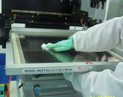
1. The operation is not in accordance with the operating specifications at the time of shipment: the circuit industry is a workshop environment, and the staff standard operation requirements are extremely strict, especially the chemical reaction environment is required in the production of circuit boards, so no impurities are allowed to penetrate. After the board spraying process is completed, the subsequent series of operations require employees to wear anti-static gloves. Because finger sweat or stains directly touch the surface, it will cause surface oxidation. If it causes defects, it is extremely difficult to find, and it is irregular. Test And the Shanghai tin experiment is difficult to show.

2. Welding defects caused by warpage: circuit boards and components warp during the welding process, and defects such as virtual welding and short circuit due to stress deformation. Warpage is often caused by the temperature imbalance of the upper and lower parts of the circuit board. The large PCB will also warp due to the drop of the board's own weight. The ordinary PBGA device is about 0.5mm away from the printed circuit board. If the device on the circuit board is large, the solder joint will be under stress for a long time as the circuit board cools down and the solder joint will be under stress. If the device is raised by 0.1mm, it is enough to cause For special products, the yin and yang jointing of the circuit board factory can be required to reduce the warpage, or to adopt the appropriate size of the imposition as far as possible, and it should not be too large or too small.
Multilayer circuit board manufacturers
3. The tin furnace used for spraying tin is not cleaned up on time: the on-time maintenance of the tin furnace is very important, because the tin spraying is a vertical cycle process, the circuit board surface will be under strong pressure, for those solder masks that are not fully dried and the characters are not firm If the board is not cleaned for too much time, it will cause surface adhesion.
4. The source of tin for incoming materials: For material procurement, some circuit board factories blindly seek to reduce costs. When using tin sprayed raw tin, the procurement industry recycles tin, or sources with unstable content, generally very low unit prices. Board manufacturers may have such a risk probability, and it is recommended that you choose suppliers carefully.
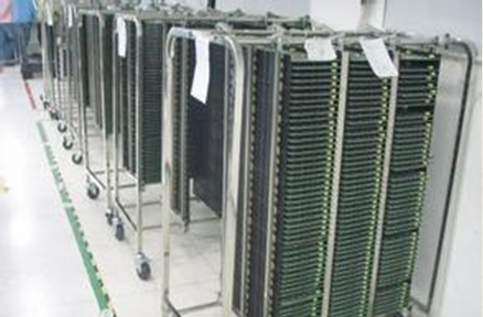
5. Storage environment and transportation: This is the link between the circuit board factory and the placement factory. Generally, there is little inventory of circuit boards, but the general inventory requires the storage environment to be dry and humid, and the packaging is complete, and it is required to be as light as possible during transportation. Handle with care. Do not allow the vacuum package to be damaged for long-term storage. The theoretical storage time of the spray tin board is one month, but the time when the solderability is better is within 48 hours. If the storage time exceeds one month, it is recommended to return to the circuit board factory for special use. Clean the potion and bake the plate. Baking parameters 150°, 1 hour.
Please combine the above PCB factory circuit as a reference