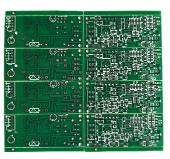
For hardware electronic product designers, PCB design is becoming more and more complicated. Advanced packaging devices with denser pins are used, and the network density per unit area is constantly increasing, which brings greater pressure on the wiring. At the same time, more engineers no longer meet the requirement of 100% routing rate of automatic routers, hoping to conduct electrical rules to constrain the wiring to meet the signal integrity requirements.
The current domestic design situation is similar, and many high-speed designs are still in the program discussion stage or prototype stage. Engineers foresee or have observed some problems, such as overshoot, undershoot, oscillation, crosstalk and other issues. However, the cause of the entire high-speed problem is not well understood with high-speed analysis and simulation methods, and high-speed digital circuit design and RF design are often treated as the same problem. I feel that in actual high-speed analysis, timing analysis is also a key to digital circuit design, but it is often overlooked. In addition to analysis, in order to reduce the transmission line effect and reduce the PCB area, the realization of high-density design is also a problem. However, in China, due to concerns about crosstalk, development cycle or commissioning issues, multiple single boards are often used to reduce the design density.
1. For high-speed PCB design, pre-simulation analysis is very important. These include device selection, model editing, signal distribution, matching strategy, and stacking design. The pre-simulation analysis can not only use the topological structure editing in the schematic diagram stage, but also must use the PCB LAYOUT tool for layout detection and pre-wiring analysis to estimate the difficulty of implementation and the wiring method. At the same time, the distributed plane layer is divided into power sources first, and the priority of the wiring layer is arranged to avoid the cross division of key signals to the greatest extent.

2. After completing the schematic diagram, the average engineer can't wait to start PCB design. It is recommended to take a day or two to check the schematic diagram. Because in the later stage, if the schematic design is found to be wrong, the cost of the change will be too great. Start PCB design, don't be busy with wiring, first lay out well. According to experience, PCB design time is generally allocated according to the three-three system, layout 1/3 time, wiring 1/3, and inspection 1/3. The layout is quite critical, and experienced engineers already have a plan for the key wiring at the same time as the layout. The layout is generally based on the big first, then the small, the key and then the second. The components with positioning requirements are placed first. In the layout, in addition to the wiring quality, issues such as testing and processing must also be considered, and various factors should be weighed.
3. Manual wiring is still the choice of most engineers, because many people are not very satisfied with the results of automatic wiring. In fact, some advanced EDA tools now have automatic wiring that is quite intelligent. Automatic wiring does not mean that it is all left to tools, and there are many places that require human intervention. Personal experience believes that network classification (class), wiring priority settings, and wiring rules are the main factors that affect the wiring rate and wiring effect.
Some people also say that PCB design is the transformation from abstract concepts to actual products. PCB design is actually a hybrid technology. The designer is required to have an understanding of all aspects of circuit board principles, electromagnetic fields, wiring algorithms, production and processing, testing, etc. Therefore, an excellent PCB copying engineer should pay attention to learning these knowledge.