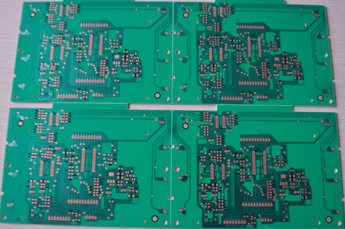
1. PCB layout
1. PCB layout refers to the reasonable layout of circuit components. What kind of placement is reasonable. A simple principle is the clear division of modularity. In other words, a person with a certain circuit foundation can see which printed circuit board is used to achieve what function.
2. Specific design steps: First, generate the initial printed circuit board file according to the schematic diagram, complete the pre-layout of the printed circuit board, determine the relative printed circuit board layout area, and then tell the structure that the structure is based on the area we give, and then According to the overall structure design, specific constraints are given.
3. According to the structural constraints, complete the drawing of the board edges, positioning openings and some prohibited cloth areas, and then complete the placement of the connectors.
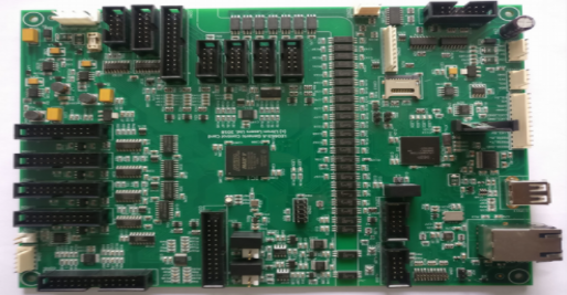
4. PCB component placement principle: Generally, the main control microcontroller (MCU) is placed in the center of the circuit board, and then the interface circuit is placed close to the interface (such as network ports, USB, VGA, etc.). ), most interfaces have electrostatic discharge protection and filtering functions. The principle to follow is to protect before filtering.

5. Then there is the power supply module. Usually, the main power module is placed at the power inlet (for example, the 5V of the system). Independent power modules (such as 2.5V provided by the module circuit) can be placed in densely populated places in the same power supply network according to actual conditions.
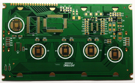
6. Some internal circuits are not connected to the connector. We usually follow such a basic principle: high-speed and low-speed partition, analog and digital partition, interference source and sensitive receiver partition.
7. Then, for a single circuit module, design according to the current flow direction during circuit design.
The whole circuit layout is like this, welcome to add and correct.
2. Wiring
1. Wiring, the most basic requirement is to ensure the effective connection of all networks. Connectivity is easy to do, and effectiveness is a vague concept. In fact, there are only two kinds of signals in the circuit: digital signals and analog signals. For digital circuits, it is to ensure sufficient noise tolerance, and for analog signals, it is to achieve zero loss as much as possible.
2. Before wiring, it is usually necessary to understand the entire PCB laminate design, that is, plan all wiring layers as: the best wiring layer and the sub-optimal wiring layer, the best wiring layer, that is, the adjacent complete grounding layer. Layers are generally used to distribute important signals (including all signals in DDR, differential signals, analog signals, etc.). ). Other signals (I2C, UART, SPI, GPIO) pass through other layers, and ensure that only the relevant signals of the circuit (such as DDR, network port, etc.). ) Exists in important areas.
3. In the high-speed signal wiring, reflection, crosstalk, electromagnetic compatibility and other issues need to be considered, so impedance matching is generally required, such as single line 50R, differential line 100R, etc. The actual design shall prevail (the principle is to ensure that the impedance is equal and continuous). Crosstalk mainly considers 3W/2W principle, group grounding treatment, etc.
4. The power supply and power circuit should first ensure sufficient carrying capacity, that is, the entire loop of the power supply should be as thick and short as possible. From the perspective of electromagnetic compatibility, the echo is called a loop, which forms a loop antenna and radiates outwards, thereby reducing the loop area as much as possible.
The overall wiring of the circuit is probably like this, welcome the great God to add and correct.
Three. Land
1. Grounding and grounding design are very important in PCB design, because grounding is an important reference plane. If there is a problem with the ground plane design, other signals cannot be stabilized.
2. Generally, we can divide it into chassis grounding and system grounding. As the name implies, the chassis ground is the ground connected to the product metal sheet, and the system ground is the reference plane of the entire circuit system.
3. The practical principle of general systems and cabinets is: the cabinet is divided into grounding and system, and then connected to high-voltage capacitors through magnetic beads or multiple points.
4. On the system: functionally, it is divided into digital, analog and power. (There has been controversy about the division of land. I come from here.)
First of all, when the layout is very reasonable, the land can be divided. The meaning of the layout is very reasonable, that is, the digital area has only digital signals, the analog area has only analog signals, and the power area has only power signals, and there is a complete ground layer below. Because electric current is very similar to electric current, they both flow downwards, and there is a complete ground plane under them, so starting from the shortest and lowest principle, they flow directly back below and will not escape to other places.
However, in some cases, it is not ideal, and there are some intersections in different areas. At this time, usually choose a single point of understanding and use OR resistors (magnetic beads are not recommended because they have a filtering effect at high frequencies). The resistance is located where the intersection is densest and the circulation area is the smallest.