The impact and requirements of different manufacturing processes on pads on PCB board
1. If the two ends of the patch components are not connected to the plug-in components, test points must be added. The diameter of the test points should be between 1.0mm and 1.5mm, so as to facilitate the online testing of the tester. The edge of the spot pad should be at least 0.4mm away from the edge of the surrounding pad. The diameter of the test pads should be more than 1mm, and network properties must be provided. The center distance between the two test pads should be greater than or equal to 2.54mm. If the hole is used as the measuring point, the welding pad must be added outside the hole with a diameter of more than 1mm (including).
2. Pads must be added where holes with electrical connections are located; All pads must have network properties. Network names must not be the same for networks without connecting components. The distance between the center of the positioning hole and the center of the test pad is more than 3mm; Other irregular shaped grooves, pads, etc., but with electrical connections, are uniformly placed in the mechanical layer 1 (refers to the grooves of single inserts, safety pipes, etc.).
3. foot spacing dense (pin spacing less than 2.0mm) component foot pad (such as: IC, swing socket, etc.) if not connected to the hand plug-in pad must be added to the test pad. The diameter of the test point should be between 1.2mm and 1.5mm, so as to facilitate the online tester test.
4. Pad spacing is less than 0.4mm, must be coated with white oil to reduce the wave peak continuous welding.

5. The ends and ends of the patch components of the dispensing process should be designed with tin lead. The width of tin lead is recommended to use 0.5mm wire, and the length is generally 2 or 3mm.
6. If the single panel has hand welding components, to drive away the tin slot,the direction is opposite to the tin direction, the width of the size of the hole is 0.3mm to 0.8mm;
7. The spacing and size of conductive rubber keys should be consistent with the actual size of conductive rubber keys. The PCB board connected with this should be designed as a gold finger,and the corresponding gold plating thickness should be specified (generally greater than 0.05um~0.015um).
8. The size and spacing of the pad should match the size of the patch component.
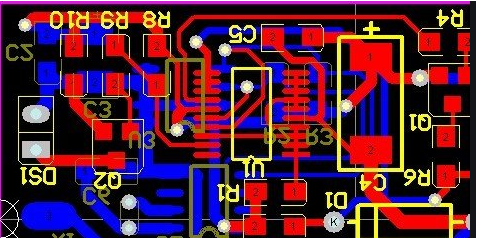
a) Without special requirements,the shape of component hole,pad and component foot must match,and ensure the symmetry of pad relative to the hole center (square element foot with square element hole,square pad;Round element foot with round element hole, round pad),and adjacent pads are kept separate,to prevent thin tin, wire drawing;
b) Separate pad holes should be provided for adjacent parts pins in the same circuit or compatible devices with different PIN spacing,especially for the connection between compatible pads of relays. If separate pad holes cannot be set due to PCB layout,the two pads must be surrounded by blocking paint.
9. Multi-layer board design should pay attention to,metal shell components, plug-in shell and printed board contact,the top of the pad can not be opened, must be covered with green oil or silk screen oil (such as bipedal crystal, 3 feet LED).
10. PCB board design and layout as far as possible to reduce the printed board slot and hole,so as not to affect the strength of the printed board.
11. Precious components: precious components should not be placed at the corners,edges,mounting holes,grooves,cutting ports and corners of PCB. These positions are high stress areas of printed board,which are easy to cause cracks and cracks of solder joints and components.
12. heavier devices (such as transformers) should not be far away from the positioning hole,so as not to affect the strength and deformation of the printed board. The heavier components should be placed at the bottom of the PCB (which is also the last side to enter the wave soldering).
13. transformers and relays and other radiation energy devices should be far away from amplifiers,single chip microcomputer,crystal oscillator, reset circuit and other easily disturbed devices and circuits,so as not to affect the reliability of the work.
14. For QFP package IC (need to use wave welding process), must be 45 degrees, and add tin.
15. SMT components over wave soldering, the board has inserted elements (such as heat sink, transformer, etc.) around and under the body of the board can not open heat dissipation hole, to prevent PCB over wave soldering, wave 1 (turbulence wave) tin stick to the upper board parts or parts feet, after the assembly of the machine foreign body.
16. A large area of copper foil is required to be connected with a separate tropical pad. In order to ensure good tin penetration, the pads of the components on the large area of copper foil are required to be connected with the pads by the insulation belt. For the pads that need to pass over 5A or more large current, the heat insulation pads cannot be used.
17. In order to avoid deviation and monument setting after reflow welding, the pads at both ends of reflow 0805 and 0805 chip components below shall ensure symmetry of heat dissipation, and the width of the connection part between the pads and printed wire shall not be greater than 0.3mm (for asymmetrical pads).