Multilayer circuit board proofing production process
Multilayer circuit boards are evolving in the direction of lighter, thinner, high-density, and multi-layer boards: coupled with the rise of wearable electronic products, the demand for flexible circuit boards has also begun to rise. All these application changes make the PCB online automatically The test system is also facing severe tests while the market demand is "blowout". The editor of Shenzhen Circuit Board Factory will introduce the production process of multi-layer circuit board proofing in detail.
1. Manufacturing negatives: due to the presence of side corrosion, the accuracy of the drawing lines must be sufficient, so certain process compensation must be made when light drawing the negatives, and the process compensation value must be determined by measuring the side corrosion values of different thicknesses cu. The negative is a negative.
2. Material preparation: Try to purchase plates with a fixed size of 300mm*300mm and a maintenance film on the Al and Cu surfaces, especially Rogers. The dielectric constant is the same as the drawing.

3. Drawing graphics:
a. Due to the pre-treatment of this process, the maintenance of the Al base needs to be stopped. There are many ways. It is recommended to use a 0.3mm thick epoxy board with the same size as the Al base board. The surrounding area should be sealed with tape and compacted to prevent the solution from infiltrating.
b. It is recommended to use chemical micro-etching for the disposal of Cu surface, which has the best effect.
c. After the Cu surface is processed, the wet film should be screen printed immediately after drying to prevent oxidation.
d. After developing, use a scale magnifying glass to measure the line width and whether the gap can reach the drawing request, to ensure that the line is lubricated and free of jagged. If the thickness of the substrate at the site is greater than 4mm, it is recommended to remove the drive roller on the developing machine to prevent the card from causing rework.
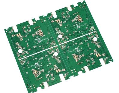
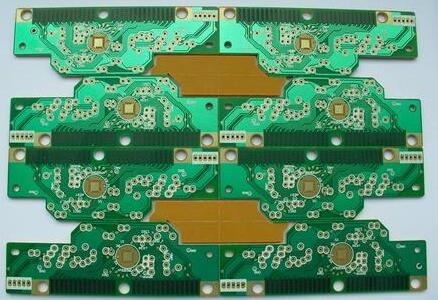
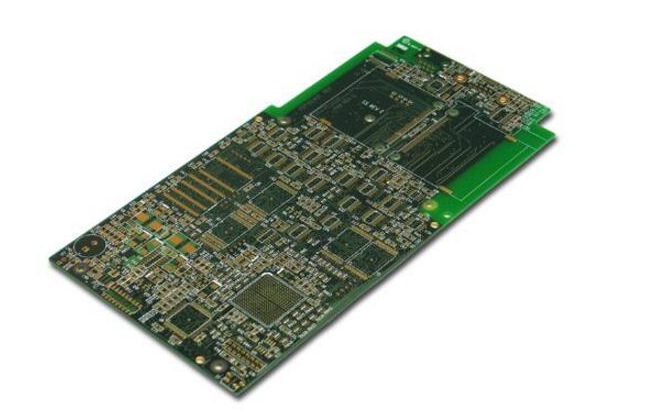
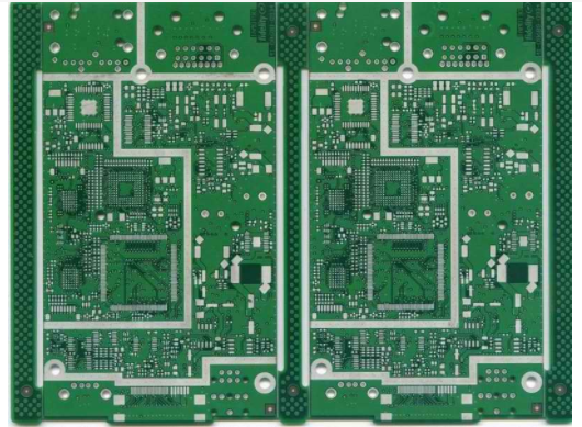
PCB multilayer board
4. Etching: Use acidic CuCl-HCl solution to etch. Use the experiment board to adjust the solution, etch the m substrate when the etching effect is the best, and turn the pattern side down to reduce the amount of side etching.
5. Surface treatment (sn immersion): After the etching process is completed, do not rush to remove the film. Immediately prepare the immersion sn solution, that is, remove the film, that is, immerse the sn. The effect is the best.
6. Machining: CNC milling machine should be used for shape processing to separate the Jusi fuyixi and Canji partly, so as to prevent the delamination caused by the difference in thermal conductivity and deformation between the two, and the graphics should be facing To reduce the generation of delamination and burrs.
ipcb is a high-precision, high-quality PCB manufacturer, such as: isola 370hr PCB, high-frequency PCB, high-speed PCB, ic substrate, ic test board, impedance PCB, HDI PCB,Rigid-Flex PCB, buried blind PCB, advanced PCB, microwave PCB, telfon PCB and other ipcb are good at PCB manufacturing.