Foreword: PCB surfacetreatment technology refers to the artificial formation of a surface layer on the PCB components and electrical connection points that is different from the mechanical, physical and chemical properties of the substrate. Its purpose is to ensure good solderability or electrical properties of the PCB. Because copper tends to exist in the form of oxides in the air, which seriously affects the solderability and electrical properties of the PCB, it is necessary to perform surface treatment on the PCB
The common surface treatment methods are as follows:
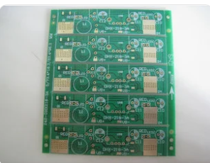
1, hot air leveling
The process of coating molten tin-lead solder on the surface of the PCB and flattening (flattening) with heated compressed air to form a coating layer that is resistant to copper oxidation and provides good solderability. During hot air leveling, the solder and copper form a copper-tin metal compound at the junction, and the thickness is about 1 to 2 mils;

2, organic anti-oxidation (OSP)
On the clean bare copper surface, a layer of organic film is grown chemically. This layer of film has anti-oxidation, heat shock resistance, and moisture resistance to protect the copper surface from rusting (oxidation or sulfidation, etc.) in a normal environment; at the same time, it must be easily assisted in the subsequent welding high temperature The flux is quickly removed to facilitate welding;
3, electroless nickel gold
A thick layer of nickel-gold alloy with good electrical properties is wrapped on the copper surface and can protect the PCB for a long time. Unlike OSP, which is only used as an anti-rust barrier layer, it can be useful in the long-term use of PCB and achieve good electrical performance. In addition, it also has tolerance to the environment that other surface treatment processes do not have;
4, chemical immersion silver
Between OSP and electroless nickel/immersion gold, the process is simpler and faster. When exposed to heat, humidity and pollution, it can still provide good electrical performance and maintain good solderability, but it will lose its luster. Because there is no nickel under the silver layer, immersion silver does not have the good physical strength of electroless nickel/immersion gold;
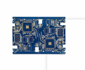
5, electroplating nickel gold
The conductor on the PCB surface is electroplated with a layer of nickel and then electroplated with a layer of gold. The main purpose of nickel plating is to prevent the diffusion between gold and copper. There are two types of electroplated nickel gold: soft gold plating (pure gold, gold indicates that it does not look bright) and hard gold plating (the surface is smooth and hard, wear-resistant, contains cobalt and other elements, and the surface looks brighter). Soft gold is mainly used for gold wire during chip packaging; hard gold is mainly used for electrical interconnection in non-soldering places (such as gold fingers).
6, PCB mixed surface treatment technology
Choose two or more surface treatment methods for surface treatment. The common forms are: Immersion Nickel Gold + Anti-oxidation, Electroplating Nickel Gold + Immersion Nickel Gold, Electroplating Nickel Gold + Hot Air Leveling, Immersion Nickel Gold + Hot Air Leveling .