Electromagnetic compatibility EMC refers to the ability of a PCB device or system to operate in compliance with the requirements in its electromagnetic environment and not produce intolerable electromagnetic interference to any equipment in its environment. On the one hand, it is necessary to reduce the emission of the electromagnetic spectrum as much as possible, and on the other hand, it is necessary to protect the equipment from electromagnetic interference. Electromagnetic interference source, coupling path and receiver are the three elements that form interference, and the lack of any one of them will not cause interference.

The electromagnetic compatibility design is closely related to the specific circuit. In order to carry out the electromagnetic compatibility design, the PCB design engineer needs to minimize the radiation (radio frequency energy leaking from the product) and enhance its radiation (the energy entering the product) The susceptibility and anti-interference ability. As for the common conduction coupling at low frequencies and the common radiation coupling at high frequencies, cutting off the coupling path must be given full attention in PCB design. There are three basic principles of PCB anti-interference design: PCB suppresses the interference source, cuts off the interference propagation path, and improves the anti-interference performance of sensitive devices.
1. PCB design suppresses interference sources
Suppressing the interference source is to reduce the du/dt (digital device voltage change rate), di/dt (digital device current change rate) of the interference source as much as possible. This is the most prioritized and most important principle in anti-jamming design, and it often has the effect of getting twice the result with half the effort. Reducing the du/dt of the interference source is mainly achieved by connecting capacitors in parallel at both ends of the interference source. Reducing the di/dt of the interference source is achieved by connecting inductance or resistance in series with the interference source loop and adding a freewheeling diode.
2. Cut off the interference propagation path
(1) Fully consider the impact of the power supply on the microcontroller. If the power supply is done well, the anti-interference of the whole circuit will be solved more than half. Many single-chip microcomputers are very sensitive to power supply noise, and a filter circuit or voltage regulator should be added to the power supply to reduce the interference of power supply noise to the single-chip microcomputer.
(2) Pay attention to the crystal oscillator wiring. The crystal oscillator is as close as possible to the pins of the microcontroller, the clock area is isolated with a ground wire, and the crystal oscillator shell is grounded and fixed.
(3) Reasonable division of the circuit board, such as strong and weak signals, digital and analog signals. Keep interference sources (such as motors, relays) away from sensitive components (such as single-chip microcomputers) as far as possible.
(4) Separate the digital area from the analog area with a ground wire, separate the digital ground from the analog ground, and finally connect it to the power ground at one point. A/D, D/A chip wiring is also based on this principle.
3. Improve the anti-interference performance of sensitive devices in PCB design
Improving the anti-interference performance of sensitive devices refers to the method of minimizing the pickup of interference noise from the side of sensitive devices and recovering from abnormal conditions as soon as possible. Common measures to improve the anti-interference performance of sensitive devices:
(1) For the idle I/O ports of the single-chip microcomputer, do not float, but should be grounded or connected to the power supply. The idle terminals of other ICs are grounded or connected to power without changing the system logic.
(2) The use of a power supply monitoring circuit for the single-chip microcomputer can greatly improve the anti-interference performance of the entire circuit.
(3) On the premise that the speed can meet the requirements, try to reduce the crystal oscillator frequency of the single-chip microcomputer and select low-speed digital circuits.
(4) IC devices should be soldered directly on the circuit board as much as possible, and IC sockets should be used sparingly.
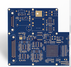
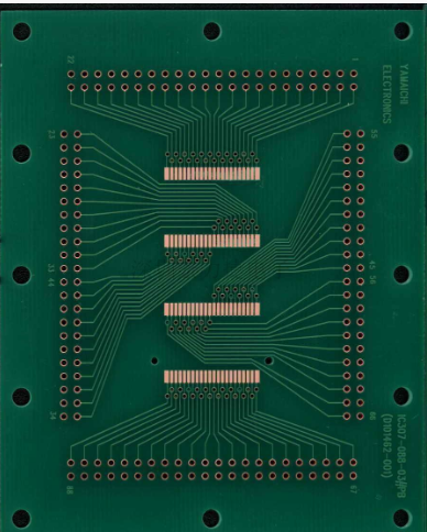
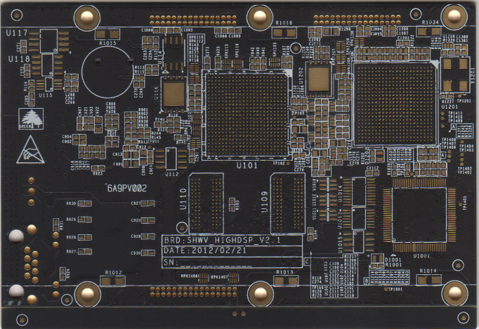
PCB proofing refers to the trial production of printed circuit boards before mass production. The main application is the process of small batch trial production of electronic engineers after designing the circuit and completing the PCB. This process belongs to the PCB proofing as we understand it before the product design is confirmed and tested.
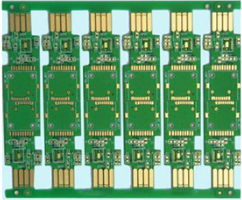
PCB proofing surface treatment generally uses hot air leveling and spraying tin, full-board nickel and gold plating, organic solderability preservative (OSP), and immersion silver
, Immersion gold, Immersion tin, electroplating hard gold, chemical nickel palladium gold and other processes to ensure good solderability or electrical properties, and these processes need to fully consider the service provider’s production strength and service level.