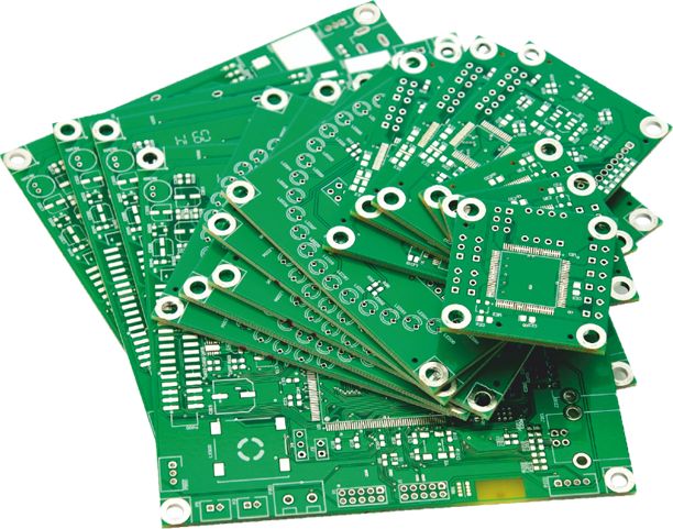
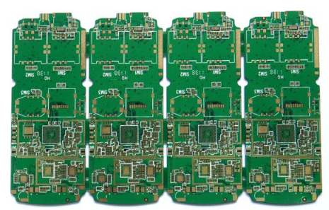
The printing line needs attention when PCB proofing:
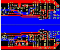
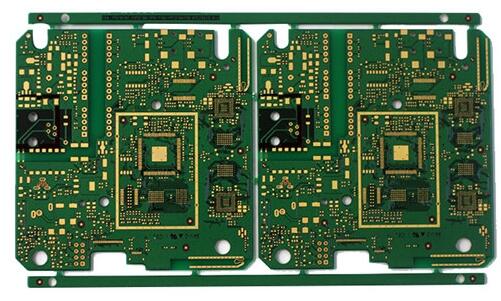
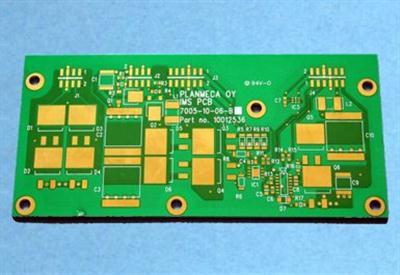
PCB printing line width: The line width should be able to meet the electrical performance requirements and be easy to produce. The minimum value should withstand the current, but the minimum value should not be less than 0.2mm. In high-density, high-precision printed lines, the line width and spacing are usually 0.3mm; in the case of high current line width, considering the temperature rise, single board experiments show that when the thickness of the copper foil is 50μm, the line width is 1~1.5 mm, with a current of 2A, the temperature rise is very small, therefore, generally 1~1.5mm wide wire can meet the design requirements without causing temperature rise. The common ground wire of PCB printed wires should be as thick as possible, and if possible, use wires larger than 2~3mm, which is especially important in circuits with microprocessors.

Because the local line is too thin, the current change, the ground potential change, and the instability of the microprocessor timing signal will worsen the noise tolerance in the inclination package of the IC pin line, you can apply 10-10 and 12- The principle of 12, that is, when two pins pass through 2 lines, the diameter of the pad can be set to 50mil, and the line width and line spacing are 10mil. When there is only one line passing between the two feet, the diameter of the pad can be set to 64mil, The line width and line spacing are 12mil.
PCB proofing and printed wire spacing: The spacing between adjacent wires must be able to meet electrical safety requirements, and in order to facilitate operation and production, the spacing should also be as wide as possible. The minimum spacing must be at least suitable for the voltage to be maintained.
This voltage usually includes working voltage, additional fluctuating voltage and peak voltage caused by other reasons. If technical conditions allow a certain degree of metal residue between the wires, the spacing will be reduced. Therefore, PCB designers should consider this factor when considering voltage.
When the PCB wiring density is low, the interval of the signal lines can be increased appropriately, and the signal lines with the difference between high and low levels should be as short as possible and increase the interval.
Shielding and grounding of printed wires: The common ground of printed wires should be arranged on the edge of the printed circuit board as much as possible. Keep as much copper foil as possible on the PCB board as the ground wire, so that the shielding effect is better than the long ground, the transmission line characteristics and shielding effect will be improved, in addition to reducing the power distribution capacity.
It is best to form a ring or net for the common ground wire of the PCB proofing printed wires, because when there are many integrated circuits on the same circuit board, especially when power consumption components are large, the ground potential difference is caused by limitations. The graph leads to a reduction in noise tolerance and when the circuit is made, the ground potential difference is reduced. In addition, the grounding and power graphics are as parallel as possible to the flow of data. This is the secret of enhancing the ability to suppress noise; multilayer PCBs can be used as shielding layers, power layers, and grounding layers can be used as shielding layers, and the inner layers of multilayer PCBs are generally Ground layer and power layer design, inner layer signal line design