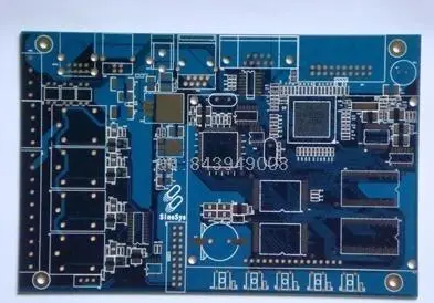
PCB copy board company circuit board mounting holes and bracket holes:
The mounting holes of the PCB board and the mounting holes of the bracket should be reserved because they cannot be routed near these holes and holes.
The rules for PCB board wiring are as follows:
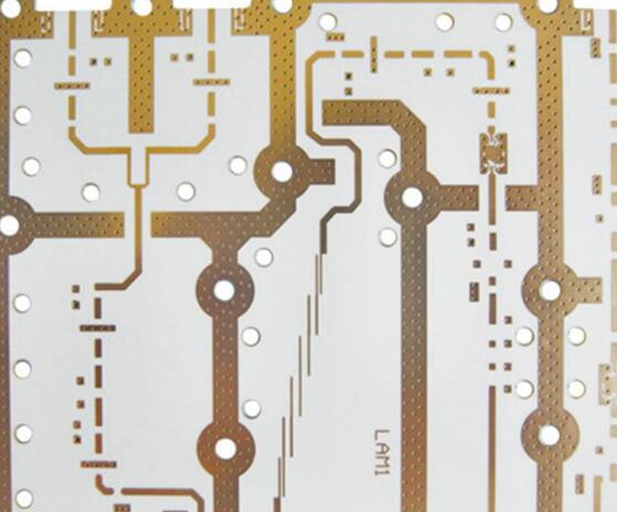
1) The length of the copper film line should be as short as possible, especially in high-frequency circuits. The corners of the copper film line should be round or inclined, and in the case of high-frequency circuits and wiring density, right angles or acute angles will affect the electrical performance.
When double-panel wiring, the two sides of the wire should be perpendicular to each other, inclined or bent, and avoid being parallel to each other to reduce parasitic capacitance.

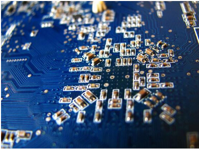
2) Line width The width of the copper film line should be able to meet the requirements of electrical characteristics, easy to produce as a standard, and its minimum value depends on the current flowing through it, but generally should not be less than 0.2mm. As long as the board area is large enough, the copper film line width and spacing are best to choose 0.3mm. Generally, a line width of 1~1.5mm is allowed to flow a current of 2A. For example, for line widths greater than 1mm, it is best to choose ground and power lines. When two lines are routed between the IC seat pads, the diameter of the pads is 50 mils, and the line width and line spacing are 10 mils. When a line is taken between the pads, the diameter of the pads is 64 mils, and the line width and line spacing are 12 mils. .
Please pay attention to the conversion between metric system and imperial system, 100mil = 2.54mm.
3) Line spacing The spacing between adjacent copper film lines should meet electrical safety requirements, and in order to facilitate production, the spacing should be as wide as possible. The minimum spacing can at least withstand the peak value of the increased voltage.
PCB copy board company in the case of low wiring density, the spacing should be as large as possible.
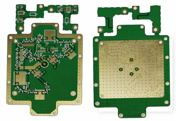
4) The common ground wire of shielding and grounding copper film wires should be placed as far as possible on the edge of the circuit board. Keep as much copper foil as the ground wire on the PCB board to enhance the shielding ability. In addition, the shape of the ground wire is preferably made into a ring or a grid.
The multi-layer PCB board uses the inner layer as a dedicated layer for power and ground, so it can play a better shielding effect.
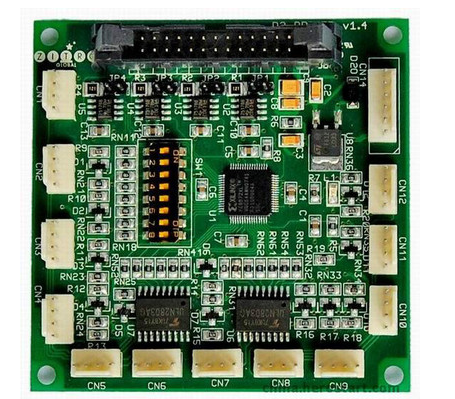
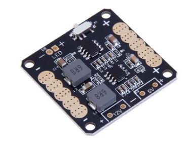
2. If there is no special requirement for the PCB copy board company according to the circuit function layout, the components should be arranged as far as possible according to the component arrangement of the schematic diagram, the signal enters from the left, the right output, and the output from the top and bottom of the input. According to the circuit flow, arrange the position of each functional circuit unit to make the signal flow smoother and keep the direction consistent. With each functional circuit as the core, around the core circuit layout, the component layout should be uniform, clean, and compact. The principle is to reduce and shorten the leads and connections between the components.
The digital circuit part should be laid out separately from the analog circuit part.
3. The distance between the components and the edge of the PCB board. All components should be placed within 3mm from the edge of the PCB board, or at least the distance from the edge of the PCB board is equal to the thickness of the board. This is due to the assembly line plug-in in mass production and wave soldering, PCB copy board The company should provide it for the use of the guide groove, and also prevent the copper film line from breaking due to the damaged shape of the PCB board edge and causing waste.
If there are too many on the PCB components, and the last resort is more than 3mm, you can add a 3mm auxiliary edge on the edge of the PCB board, on the auxiliary edge of the V-shaped groove, in the production of manual opening.
4. The sequence of component placement First place the components in a fixed position that is closely aligned with the structure, such as power sockets, LEDs, switches and connection plugs. Place special components, such as heating elements, transformers, integrated circuits, etc.
Finally, place small parts such as resistors, capacitors, diodes, etc.