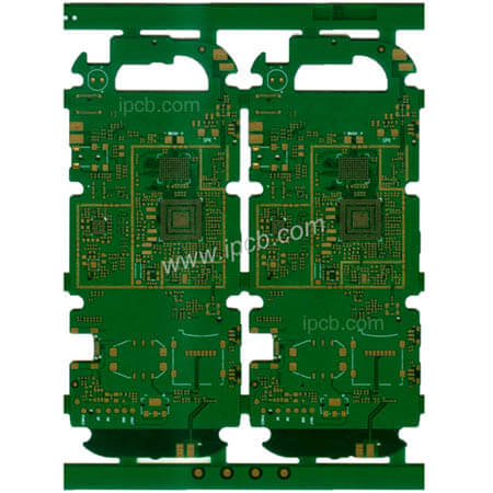
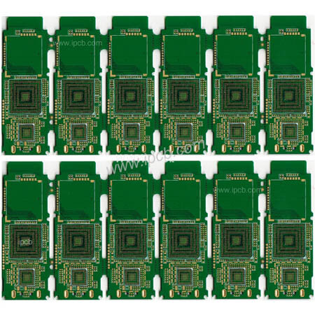
1. The outer frame (clamping edge) of the PCB board adopts a closed-loop design to ensure that the PCB board will not be deformed after being fixed on the fixture.
2. The width of the PCB board is less than 260 mm (Siemens line) or less than 300 mm (Fuji line). If automatic dispensing is required, the width of the PCB board is less than 125 mm * 180 mm.
3. The PCB layout is as close to a square as possible. It is recommended to use 2 x 2, 3 x 3,... puzzles; but don’t fight yin and yang.
4. The center distance between the small plates is controlled between 75 mm and 145 mm.

5. When setting the reference positioning point, usually leave a resistance-free welding area 1.5 mm larger than the positioning point.
6. There should be no large equipment or protruding equipment near the connection point between the outer frame of the panel and the inner panel, and between the panel and the panel. The distance between the component and the PCB should be greater than 0.5mm. Ensure the normal operation of the tool;
7. There are four positioning holes on the four corners of the outer frame of the panel. The diameter of the hole is 4 mm (+0.01 mm). The strength of the holes should be moderate to ensure that there is no break between the upper and lower plates. The hole position has high precision, and the hole wall is smooth and free of burrs;
8. Each small PCB board must have at least three positioning holes, with a diameter of 3<6 mm, and no wiring or repair of 1 mm edge positioning holes.

9. The entire circuit board is positioned as PCB, and the reference symbol is positioned as a fine-tuning component. In principle, QFPs with a spacing of less than 0.65 mm should be set in the diagonal position, and the positioning reference symbols of the PCB daughter board should be matched. Use and place it on the diagonal of the positioning component.
10. Large components should be equipped with positioning posts or holes, such as I/O ports, microphones, battery ports, micro switches, earphone ports, motors, etc.