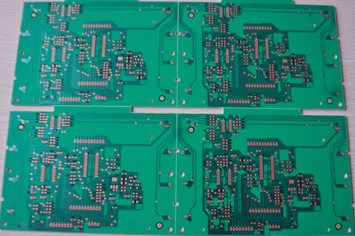
Vias, also known as metallized holes, are indispensable in double-sided PCBs and multilayer PCBs.
In order to connect the wires or planes of the same network between the layers, a via hole needs to be drilled at the intersection of the wires or copper foil planes between the different layers, and the copper foil is plated in the hole wall by electroplating to allow the wires to pass through this The metalized vias are connected together, which can be said to be very useful.
Compared with the pads of the plug-in components, the vias do not have a soldering layer, that is, the pads of the vias are usually covered with insulating ink.
Of course, some manufacturers with relatively rough processes directly expose the via pads, so when components are soldered, especially on automatic SMT lines, other impurities such as tin beads may adhere to them and cause short circuits.
In multi-layer boards, vias can be not only through holes, but also blind holes and buried holes.
Vias, that is, vias pass through all the wiring layers of the circuit board, and of course, they can also connect the wiring of all electrical layers.
Blind vias, vias that connect traces on the surface to the traces on the inner layer, can be seen from one side, but not on the other side.
Buried vias are vias that connect the wiring layers between the inner layers. Buried vias are called buried vias because they are buried inside the circuit board. This type of hole is invisible on the surface of the circuit board.
Through holes are usually mechanically drilled, blind holes often need to be drilled on the pad, so the size is small, usually laser drilling, and buried holes may have both forms.
Note: Multi-layer board blind buried vias need to consider the PCB manufacturing process and laminate design. According to the different layers of blind buried vias, they are also divided into first-order, second-order and multi-stage blind-buried vias. The more the number of stages, the more the manufacturing process. Complexity, the cost will be greatly increased; so if the circuit board must use blind and buried vias, if you do not know the manufacturing process of the multilayer board before designing, please contact the manufacturer first to choose a suitable laminated structure .
The main parameters of the via hole are the inner diameter, that is, the size of the hole; the outer diameter, that is the size of the pad; the copper thickness of the hole wall, that is the thickness of the electroplated copper in the hole
So how do we choose suitable parameters for drilling holes on the circuit board-drilling size and copper foil thickness?
Most of the layout engineers who are new to the industry may say that they are selected based on the process capability of the PCB manufacturing industry.
Searching on the Internet, the minimum mechanical via can be 0.2mm, so I chose 0.2mm as my via size.
At first glance, there seems to be no problem. However, from another perspective, we all know that PCB Layout has a very important rule regarding wiring, and the shortest wiring between two points. Do you strictly follow this to review your design?
If the traces are not the shortest, why should the vias be the smallest?

The industry’s process capability can achieve a minimum aperture of 0.2mm, but there are many restrictions. For example, if the thickness of the board is less than 1.0mm, your board requires 1.6mm or even 2.0mm. You can also choose the aperture of 0.2. This Under the circumstances, the production will cause damage and serious waste of the CNC drill bit, the yield rate is low, and the manufacturing cost may be doubled because the via is too small, or even unable to produce...
Even if your sheet thickness meets the requirements, let's take a look at the actual situation of the production line.
The production process of the circuit board is to open the material, drill, and then cover the conductive film after multiple processes, electroplating...so that the copper foil that meets the thickness is evenly distributed in the hole.
If you choose a via with an inner diameter of 0.2mm, then from the manufacturing process, because the conductive film and electroplated copper need to occupy a part of the space, in order to achieve the finished hole diameter of 0.2mm, you need to use a CNC drill bit larger than 0.2mm, generally 0.25mm The size of the drill bit achieves a finished product size of 0.2mm.
If the board density is relatively high, there are traces or copper foil around the vias, and their spacing is smaller than the size of the CNC drill bit, the factory will have to do the necessary processing on your gerber in order to drill the hole, and the responsible manufacturer will help you Remove the surrounding wiring, and the manufacturer who is not responsible for cutting the copper directly, so that your carefully designed wiring path, wiring width and wiring spacing may all be changed due to manufacturing, and the result is that the circuit board made cannot meet the design. Requirement, the result of hardware debugging does not meet the original intention of the design...
In the end, a variety of inexplicable problems will appear in the product, and you don’t know that all of this is due to a parameter selection you took for granted.
Uh, is this the legendary butterfly effect?
PCB layout is really not just hard work, hardware engineers will be forced into hard work philosophers, is there anything?
Therefore, in order to ensure the yield and low cost of our PCB products, in terms of PCB Layout parameter settings, try not to challenge the manufacturing process limits. As for the progress of science and technology and social development, it is good to leave the work of the corresponding equipment manufacturers to complete, we As long as my product meets the design requirements when it is manufactured.
So, how to set our via parameters?
First of all, consult the cooperating supplier, the factory will give you appropriate suggestions, and add 0.1-0.2mm appropriately based on the factory's suggestion, to prevent the need to reduce costs in the future due to process restrictions and the supplier cannot be replaced;
Secondly, according to the actual situation of the project, for a board with a high PCB space density, I would rather increase the board layer, because a reasonable increase in the board layer and layout can make the electromagnetic compatibility (EMC) of the product better.
Third, for the POWER and GND vias that need to pass large currents, increase the size by 0.1-0.2mm (mainly to expand the copper foil area of the vias, which is equivalent to widening the via traces), and use multiple vias to connect Way.