PCB provides a very useful function, which is automatic push. When we manually the PCB route, we fully control the printed board and turn on the automatic push function, which will find it very convenient.
But if you want to automatically wire after the pre-wiring is completed, it is best to ensure the pre-arranged line, otherwise the software will think that this line segment can be moved, and your work will be completely overturned, resulting in unnecessary losses
4. Adding positioning holes Our printed circuit boards usually need to add some mounting positioning holes, but for POWERPCB, this is a device different from the schematic diagram and needs to be completed in eco mode. But if in the final check, the software brings us many errors, it is not very convenient.
In this case, the positioning hole device can be set to non-eco registration. Under the "Edit Device" window, select the "Edit Electrical Properties" button, in which the normal item is selected and the ECO registered item is not selected.

In this way, during the inspection, POWERPCB believes that there is no need to compare the device with the netlist, and there will be no errors that shouldn't occur.
5. Add a new power pack. Because our international and American software companies are not very compliant with the standards, we try to equip the international library for everyone to use.
But the new symbols for power and ground must be added to the library included with the software, otherwise it will not be assumed that the symbol you build is a power source. Therefore, when we want to build a power symbol that complies with GB, we need to open the existing power symbol group, select the "Edit Electrical Connection" button, click the "Add" button, and enter the name of the new symbol and other information. Then, select the "Edit Door Encapsulation" button, select the symbol name just created, draw the desired shape, exit the drawing state, and then save.
You can pull out this new symbol in the schematic.
6. Setting of empty pins In the equipment we use, some pins themselves are empty pins and are marked as NC. When we build a library, please take care, otherwise the pins marked as NC will be connected together. This is because you built NC pins in "Singal_pins" when you built the library, and POWERPCB the pins in "singal_pins" are implicit default pins, these pins are useful pins, such as VCC and GND .
Therefore, if NC pins, they must be deleted from "singal_pins", or more precisely, you don't have to ignore it at all, there is no special definition.
7. Transistor pin control The packaging of transistors has changed a lot. When we build our own transistor library, we often find that the connection from the Web table to the PCB schematic diagram is inconsistent with the connection we want.
The problem lies mainly in the construction of the database. Since transistor pins are usually marked with e, b, c, when creating your own transistor library, select the "Include text numbered pins" check box in the edit electrical connection window, and the text numbered pins tab will light up When input into the label, the corresponding pin of the transistor becomes a letter.
In this way, the PCB package corresponding to the connection will be easier to identify.
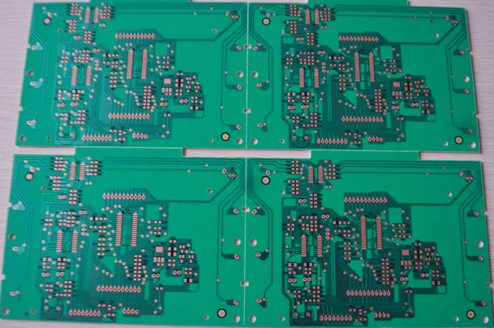
8. Pretreatment of PCB surface sticker device Now, due to the need for miniaturization, surface paste devices are becoming more and more used. In the layout process, the handling of the surface sticking device is very important, especially when the cloth multilayer board is used. Because the surface sticker only has an electrical connection on one layer, unlike the double-row in-line device placed on the board, which has a through hole, when the other layer needs to be connected to the surface device, pull a short line of the surface sticker device pin and punch a hole, And then connect with other devices, called fan-in (fan-in),
Fan-out (fan-out) operation. If necessary, we should first fan the surface sticker, fan out operation, and then wire, because if we just select fan entry and fan out operation in the automatic wiring setting file, the software will do this during the wiring process, and then pull The exit line will be tortuous and relatively long. Therefore, we can complete the PCB layout, first enter the automatic wiring device, select only fan-in and fan-out operations in the setup file, and do not select other wiring options, so the line drawn from the surface sticker is shorter, but it is also cleaner.