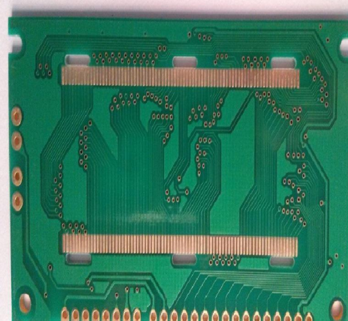
The characteristic impedance value in the PCB transmission line must match the electronic impedance of the Driver and Receiver
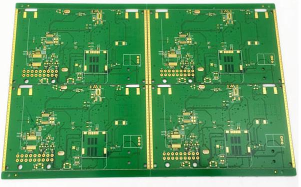
In recent years, with the improvement and application of IC integration, its signal transmission frequency and speed are getting higher and higher. Therefore, in the printed board wire, after the signal transmission (emission) reaches a certain value, it will be affected by the printed board. The influence of the wire itself, resulting in severe distortion or complete loss of the transmitted signal. This shows that the "thing" "circulated" by the PCB wire is not current, but the transmission of square wave signals or pulses in energy. The resistance encountered during transmission of the above-mentioned "signal" is also called "impedance", represented by the symbol Z0. Therefore, it is not enough to solve the problems of "on", "broken" and "short circuit" on the PCB wires, but also to control the impedance of the wires.
((A)) What is impedance?
Impedance is a parameter used to evaluate the characteristics of electronic components. The definition of impedance is the total resistance of the component to alternating current at a given frequency.

((B)) Why do we need impedance control?
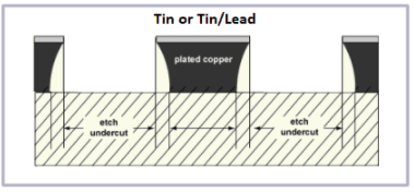
Because the characteristic impedance value in the PCB transmission line must match the electronic impedance of the Driver and Receiver, otherwise it will cause reflection and attenuation of the signal energy, and delay of the signal arrival time. In severe cases, it cannot be judged independently and booted. When the signal in the circuit board line propagates, the factors that affect its "characteristic impedance" are the cross-sectional area of the line, the thickness of the insulating material between the line and the ground layer, and its dielectric constant. The most part that affects impedance is: 1. line width, 2. pp thickness, 3. dielectric value (FR-4 = 4.3), followed by solder mask thickness, undercutting, copper thickness, etc. These will change the distribution of magnetic lines of force, and then change For the variable of assembly resistance, first understand the tolerance value requirements of assembly resistance, and then inversely infer the maximum tolerance value of the process, and calculate whether it can be achieved by software. The focus of PCB manufacturing process control is to use the material/wire diameter tolerance within 10%/the thickness of the interlayer after pressing is within 10%, and then the design requirements can be met.
((C)) What is Er value?
Generally, the dielectric constant or relative permittivity is the electrostatic energy that can be stored per unit volume of insulating material under each unit of potential gradient. If the dielectric constant is high, a lot of signal transmission is stored in the plate, which causes poor signal and slows down the propagation rate. Generally, PTF ((Teflon)) is limited to those with high signal quality requirements because its Er=2.5.
(4) General impedance is divided into 3 categories:
1. Characteristic impedance (impedance).
If the customer controls the impedance of the 4-layer board and the outer line width, the software mode for calculating the outer line width impedance is as follows.
(5) Notes for coupon design:
1. The general impedance design has a design layer (circuit layer) and a reference ground layer (corresponding layer). If the customer has no specifications, the specifications of the 4-layer board are L1 (design layer)-L2 [L2 ground layer (corresponding layer) ], L3[L3 ground plane (corresponding layer)-L4 (design layer).
2. Pay attention to the impedance control of the inner layer of the PCB. For example, two consecutive layers are controlled by the line width, and there is no other layer [ground layer copper foil (corresponding layer)]. A test that affects the impedance value.
3. Generally, the outer impedance line width needs to be protected by copper strips. The width of the copper strips is "the wider the better", and the spacing needs to be min 10 mil or more.
4. PCB inner wiring layer, if there is impedance control, you need to pay attention to its upper and lower ground layers (corresponding layers), whether it is covered with copper foil, the impedance calculation software and the impedance bar design are different.