As the functions of electronic products are becoming more and more powerful, the requirements for portability are getting higher and higher, and the miniaturization of circuit boards has become a research topic for many electronic design companies. This article takes the methods, challenges and trends of circuit board miniaturization design as the main line, combined with the powerful functions of Cadence SPB16.5 in circuit board miniaturization design, and comprehensively analyzes the engineering realization of circuit board miniaturization design. It mainly includes the following content: the current status and trends of circuit board miniaturization design, and the current mainstream HDI processing technology, introducing the latest ANYLAYER (any level) technology design method and process realization, introducing the application of embedded resistance and embedded capacitance, and embedding The design method and process realization of style components. At the same time, it introduces the support of Cadence SPB16.5 software to the miniaturization design of circuit boards. Finally, it introduces the application of HDI design in high-speed and simulation methods, the application of HDI in communication system products, the comparison of HDI and back drilling, etc.
1 Introduction
The benefits of product miniaturization are obvious, which has led to the development of circuit board miniaturization design technology.
2. HDI technology and process realization

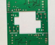
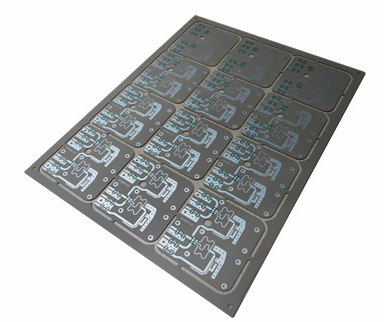
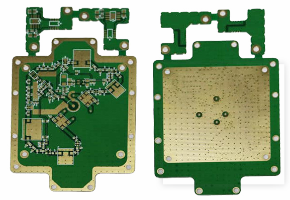
HDI: High Density Interconnect, high-density interconnection. The traditional PCB board drilling is affected by the drill, when the drilling hole diameter reaches 0.15mm, the cost is already very high, and it is difficult to improve again. The drilling of HDI boards no longer relies on traditional mechanical drilling, but a combination of laser drilling and mechanical drilling. HDI is what we usually call blind buried via technology. The emergence of HDI technology has adapted and promoted the development of the PCB industry. This makes it possible to arrange denser BGA, QFP, etc. in the PCB board.
2.1 Classification of HDI
The classification of HDI is explained in detail on IPC-2315. Here we divide it into the following types according to the depth of the laser hole: first-order HDI, second-order HDI and third-order HDI.
The first-order HDI technology refers to a hole-forming technology in which blind holes only connect the surface layer and the adjacent secondary outer layer. Usually laser holes and discs use 4/12mil (5/12mil), of course, now you can also use smaller discs such as 4/10mil to deal with higher density wiring. We generally use ordinary holes for the blind holes of the inner layer. The second-order HDI technology is an improvement and improvement on the first-order HDI technology. It includes laser blind holes directly drilled from the surface layer to the third layer (2+N+2), and the surface layer is drilled to the second layer and then from the third layer. There are two types of drilling from the second layer to the third layer (1+1+N+1+1), and the processing difficulty is far greater than that of the first-order HDI technology. The processing and manufacturing process of the third-order HDI board is basically similar to that of the second-order, except that there are several types of holes. At present, the domestic second-order HDI design and processing have been very mature.
2.2 Challenges in HDI board design
The design of multi-level HDI requires a flexible and powerful constraint manager that can identify micro-holes and ordinary mechanical holes, and can set the spacing constraints between micro-holes and other elements. The constraint relationship of the network with the same name becomes complicated, and it is necessary to support the check of the spacing constraint of the network with the same name in various situations. Need to be able to clearly display different types of via information to facilitate management by design engineers.
3. ANYLAYER (any order) technology
In recent years, in order to meet the miniaturization needs of some high-end consumer electronic products, the integration of chips has become higher and higher, the BGA pin pitch is getting closer and closer (less than or equal to 0.4 pitch), and the PCB layout has become more and more compact. Density is also increasing. In order to improve the layout rate of the design without affecting the signal integrity and other performance, the ANYLAYER (any order) technology is born. This is the arbitrary via technology (ALIVH-Any Layer IVH Structure Multilayer Printed Wiring Board). ).
3.1 Technical characteristics of via holes in any layer
Comparing the characteristics of any layer via technology with HDI technology, the biggest advantage of ALIVH is that the design freedom is greatly increased, and holes can be punched between layers at will, which cannot be achieved by HDI technology.
3.2 Design Challenges of Vias in Any Layer
Any layer via technology completely subverts the traditional via design method. If different layers of vias still need to be provided, it will increase the management difficulty. The design tool is required to have the ability of intelligent punching, and at the same time can be combined and split at will
4. Buried resistance, buried capacitance and buried components
High-speed access to the Internet and social networks requires high integration and miniaturization of handheld devices. At present, it relies on the most advanced 4-N-4 HDI technology. However, in order to achieve higher interconnection density in the next generation of new technologies, in this field, embedding passive or even active parts into PCBs and substrates can meet the above requirements. When you design mobile phones, digital cameras and other consumer electronic products, considering how to embed passive and active parts into PCBs and substrates is the best choice for current design. This method may be slightly different because you use different vendors. Another benefit of embedding parts is that the technology provides protection of intellectual property rights and prevents so-called reverse design. Allegro PCB Editor can provide the best industrial-grade solutions. Allegro PCB Editor can also work more closely with HDI boards, flexible boards and embedded parts. You can get the correct parameters and constraints to complete the design of embedded parts. The design of embedded devices not only simplifies the subsequent SMT process, but also greatly improves the cleanliness of PCB products.
5. Application of HDI design in high speed and simulation method
With the development of high-speed serial bus technology, the signal transmission rate continues to increase, and the impact of via parasitic parameters has also been paid more and more attention. High-speed simulation engineers pay attention to via optimization and use various methods to reduce the impact of via parasitic parameters. HDI can reduce the parasitic parameters of the surface device due to the design requirements of the hole in the disk. At the same time, the inductance and capacitance of the microvia are only about one-tenth of that of a standard via.