1. Software technology
After scanning the original PCB board, according to the original image, it is necessary to use the PCB copying software to complete the file map.
In terms of software type, we have a fully functional board copy software, which is very important because the choice of software can be reflected in the final exported PCB electronic layout and the resulting schematic diagram.
After choosing a well-functioning software, in order to ensure the perfect effect, for the copying of double-layer boards and multilayer boards, technically you should also have rich experience and skilled skills. Due to the same double-layer or multilayer PCB board, the holes are in the same position, but the circuit connections are different. Then, when drawing the wiring rules of the original board in the copying software, stack the top-level PCB file copied from the double-layer board on the scanned image of the other layer. Display, draw the circuit of another layer according to the position of the via, so that the exported PCB file contains the data of both sides of the double panel.

Multilayer board is the same, but after tracing the surface PCB file map, the surface layer needs to be polished with sandpaper to expose the inner layer wiring rules, and then copy it out with the same technique with the help of copying software.
Advanced scanning technology, coupled with mature software operation skills, strictly follow the process of copying the board, you will find that the exported PCB file diagram or PCB electronic layout is in the wiring rules, via position, line direction and other parameters Will be consistent with the original PCB board. On the contrary, errors in any link in the middle, whether it is the accuracy setting of the scanning process, or the judgment and description of the routing rules and functional modules of the copy board software, will affect the effect of the final PCB file.
2. Scanning process
Since PCB copy board involves a problem of copy board accuracy, for circuit boards with high precision requirements such as mobile phone boards, it is necessary to copy out high-precision PCB layouts. In the scanning process, the scanner needs to be accurately selected and set. First, ensure the accuracy of the original scanned image. It can be said that the accuracy of the copy board mainly depends on the original scanning accuracy.
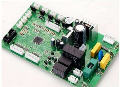
In the PCB copying process, PCB scanning is undoubtedly the first step of all processes. To get a good PCB board, it must be scanned by a computer first, and the relevant parameters and the original PCB layout must be backed up.
After disassembling the board, get the split PCB light board and formally enter the stage of copying the board. The first thing to do is to scan to store and record the PCB image. One thing to mention here is that in order to ensure that the relevant parameters on the PCB are clearly visible after scanning, the stains and residual tin on the surface of the PCB should be removed before scanning.
Here, it is necessary to introduce a concept of DPI. The meaning of DPI is the number of dots per inch. That is to say, the distance between every two points on the scanned image is 1000/DPI, the unit is mil. Then, in the mobile phone board copying, the DPI is set to 1000 when the PCB is scanned, and the distance between two points on the image is 1000/1000=1mil, which means that the accuracy at this time is 1mil.
It should be noted that the higher the accuracy of the scanned picture, the larger the picture and the higher the hardware requirements. Therefore, the DPI setting needs to be set according to the specific situation of the original board to ensure that the next steps in the copying process can be Play the best results.
Three, the detection file map
The test should also include the test of the electronic technical performance of the PCB board to ensure that it is consistent with the original board function. For the completed file diagram, in order to ensure the specification, it should be tested in the last step. A double-panel file image detection method is to use a laser printer to print the surface two-layer file image on a transparent film, and then compare the film with the original board to check whether they are consistent.