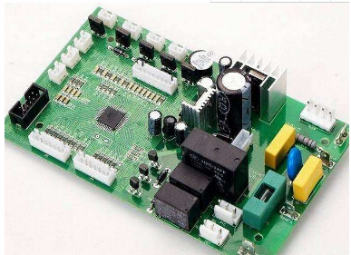
In the production process of electronic products, there will be a printed circuit board production process. Printed circuit boards are used in electronic products in all industries. It is the carrier through which the electronic schematic diagram can realize the design function, turning the design into a physical product.
The process of PCB production is like this:
Cutting -> Dry film and film -> Exposure -> Development -> Etching -> Stripping -> Drilling -> Immersion copper plating -> Solder mask -> Silk screen -> Surface treatment -> Forming -> Electrical measurement, etc. These steps
You may not know these terms yet, so let's tell you about the production process of the double panel.
One, open material
Cutting is to cut the copper clad laminate to make it into a board that can be produced on the production line. It will definitely not be cut into small pieces like the PCB diagram you designed. It is to put together a lot of pieces according to the PCB diagram, and then cut the material. After the PCB is completed, cut into small pieces.

Dry film and film
This is to paste a layer of dry film on the copper clad board. This film is irradiated with ultraviolet rays, and it will be cured to form a protective film on the board. This facilitates subsequent exposure and etches away unnecessary copper.
Then paste the film diagram of our PCB diagram. The film diagram is like a black and white negative of the photo, which is the same as the circuit diagram drawn on the PCB.
The function of the film negative is to prevent the ultraviolet light from passing through the place where copper needs to be left. As shown in the picture above, the white one is not transparent, and the black one is transparent and can transmit light.
exposure
Exposure. This exposure is to irradiate ultraviolet rays to the copper clad laminate attached to the film and dry film. The light passes through the black and transparent part of the film and hits the dry film. The dry film is cured when the light hits, and the light is not exposed. The place is the same as before.
Development is to use sodium carbonate (called developer, which is weakly alkaline) to dissolve and wash off the unexposed dry film. Because the exposed dry film is cured, it will not be dissolved, but still remains.
Etching
In this step, the unnecessary copper is etched away, and the developed board is etched with acid copper chloride. The copper covered by the cured dry film will not be etched away, and the uncovered copper will be etched. Lost. The required lines are left.
Film removal
The step of removing the film is to wash off the cured dry film with sodium hydroxide solution. During development, the uncured dry film is washed off, and the uncured dry film is washed away when the film is removed. Different solutions must be used to wash the two forms of dry film. Up to now, the circuits that reflect the electrical performance of the circuit board have been completed.
drilling
If a hole is punched in this step, the punching includes the hole for the pad and the hole for the through hole.
Immersion copper, electroplating
This step is to plate the hole wall of the pad hole and the via hole with a layer of copper and the upper layer, and the lower two layers can be connected through the via hole.
Solder mask
Soldering mask is to apply a layer of green oil to the place that is not soldered, which is not conductive to the outside world. This is through the screen printing process, and the green oil is applied, and then the process is similar to the previous process, light exposure, development, and soldering. The pad is exposed.
Silk screen
Silk-screen characters are printed on the component label, LOGO, and some descriptive text through the method of silk-screen printing.
Surface treatment
This step is to do some treatment on the pad to prevent the copper from oxidizing in the air, mainly hot air leveling (that is, tin spraying), OSP, gold immersion, gold, gold fingers and other processes.
Electrical testing, sampling, packaging
After the above production, a PCB board is ready, but the finished board needs to be tested. Whether there is an open or short circuit, it will be tested in an electrical testing machine. After this series of processes, the PCB board is formally finished, ready to be packaged and shipped.
The above is the production process of PCB, do you understand it? For multi-layer boards, a lamination process is still needed. I won't introduce it here. Basically, the process is known, and it should have some impact on the production process of the factory.