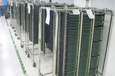
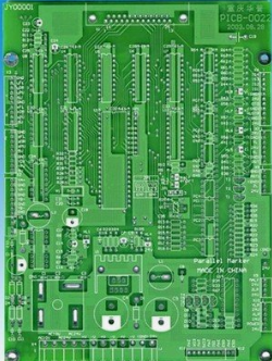
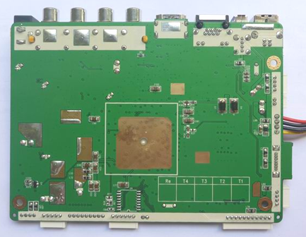
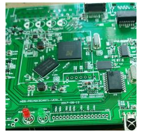
What we say to do is to turn the designed schematic diagram into a real PCB. Please don't underestimate this process. There are many things that can work in principle but can't be realized in engineering, or others can't, so it's not difficult to make a good PCB, but it's not easy to make a good PCB.
The two major difficulties in the field of microelectronics are the processing of high-frequency signal and weak signal. In this aspect, the level of PCB production is particularly important. The same principle design, the same components, different people make PCB circuit board with different results, so how to make a good PCB circuit board? Based on our past experience, I would like to share my views on the following aspects:
1, Clear design objectives
To receive a design task, first of all, it is necessary to clarify the design goal, which is the ordinary PCB, high frequency PCB, small signal processing PCB or both high frequency and small signal processing PCB. If it is an ordinary PCB, as long as the layout and wiring are reasonable and neat, and the mechanical size is accurate, such as medium load line and long line, It is necessary to adopt certain means to reduce the load, strengthen the drive for the long line, and focus on preventing the reflection of the long line.
When there are more than 40MHz signal lines on the board, special consideration should be given to these signal lines, such as crosstalk between lines. According to the distributed parameter network theory, the interaction between high speed and its connection is the decisive factor, which can not be ignored in system design. With the increase of gate transmission speed, the opposition on the signal line will increase correspondingly, and the crosstalk between adjacent signal lines will increase proportionally. Generally, the power consumption and thermal dissipation of high-speed circuit are also very large, which should be paid enough attention to when making high-speed PCB.
When there are weak signals of millivolt level or even microvolt level on the board, special attention should be paid to these signal lines. Because the small signal is too weak, it is very easy to be interfered by other strong signals. Shielding measures are often necessary, otherwise the signal-to-noise ratio will be greatly reduced. As a result, the useful signal is submerged by noise and cannot be extracted effectively.
2, Understand the functional requirements of the components used for layout and wiring
We know that some special components have special requirements in layout and wiring, such as the analog signal used in lo and APH, and the analog signal amplifier requires stable power supply and low ripple. The analog small signal part should be far away from the power device as far as possible. On the OTI board, the small signal amplification part is specially equipped with a shielding cover to shield the stray electromagnetic interference. The glink chip used into OTI board adopts ECL process, which consumes a lot of power and generates a lot of heat. Special consideration must be given to the problem of heat dissipation in the layout. If natural heat dissipation is adopted, the glink chip should be placed in a place with smooth air circulation, and the heat released can not have a great impact on other chips. If the board is equipped with horn or other high power devices, it may cause serious pollution to the power supply, which should also be paid enough attention
3, Consideration of component layout
The first factor to be considered in the layout of components is the electrical performance. The components with close connection should be put together as far as possible. Especially for some high-speed lines, the layout should be as short as possible, and the power signal and small signal devices should be separated. On the premise of meeting the circuit performance, the components should be placed neatly, beautiful and easy to test. The mechanical size of the board and the location of the socket should also be carefully considered.
In high-speed system, the grounding and transmission delay time of interconnection line are also the first factors to be considered in system design. The transmission time on the signal line has a great influence on the overall system speed, especially for the high-speed ECL circuit. Although the block itself has a high speed, the system speed can be greatly reduced due to the increase of the delay time caused by the common interconnect on the backplane (there is about 2ns delay per 30cm line length), It is better to put the synchronous counter on the same board, because the delay time of signal transmission to different boards is not equal, which may cause the shift register generator error. If it can not be put on one board, the length of clock lines from the common clock source to each board must be equal where synchronization is the key.
4, Consideration of wiring
With the completion of otni and star network design, there will be more boards with high-speed signal line above 100MHz to be designed. Here are some basic concepts of high-speed line.
Transmission line:
Any "long" signal path on the printed circuit board can be regarded as a kind of transmission line. If the transmission delay time of the line is much shorter than the rise time of the signal, the reflection of the main signal generated during the rise time of the signal will be submerged. For most MOS circuits, the ratio of rise time to line delay time is much larger, so the line length can be measured in meters without signal distortion. For fast logic circuits, especially ultra-high speed ECL.
There are two ways to make the high-speed circuit work on a relatively long line without serious waveform distortion. TTL adopts Schottky clamp method for the fast falling edge, so that the overshoot is clamped at a level one diode voltage drop lower than the ground potential, which reduces the back pulse amplitude, and allows overshoot at the slow rising edge, But it is attenuated by the relatively high output impedance (50-80 Ω) of the circuit in the state of level "H". In addition, due to the high immunity of level "H" state, the recoil problem is not very prominent. For HCT series devices, if Schottky diode clamping and series termination method are used, the improvement effect will be more obvious.
When there is a fan out along the signal line, the TTL shaping method described above appears to be insufficient at higher bit rate and faster edge rate. Because there are reflection waves in the line, they tend to synthesize at high bit rate, resulting in serious signal distortion and low anti-interference ability. Therefore, in order to solve the reflection problem, another method is usually used in ECL system: line impedance matching method. In this way, the reflection can be controlled and the integrity of the signal can be guaranteed.
Strictly speaking, for conventional TTL and CMOS devices with slower edge speed, transmission lines are not very necessary. For high-speed ECL devices with faster edge speed, transmission lines are not always needed. However, when using transmission lines, they have the advantages of predicting line delay and controlling reflection and oscillation by impedance matching.
1. Basic factors to decide whether to use transmission line or not:
(1) Along the rate of the system signal, (2) connection distance, (3) capacitive load (fan out), (4) resistive load (line termination mode)( 5) Allowable percentage of recoil and overshoot (reduction of AC immunity).
2. Several types of transmission line
(1) Coaxial and twisted pair: they are often used for system to system connections. The characteristic impedance of coaxial cable is usually 50 Ω and 75 Ω, and that of twisted pair is usually 110 Ω.
(2) Microstrip line on printed circuit board: a microstrip line is a strip conductor (signal line). It is separated from the ground plane by a dielectric. If the line's thickness, width and distance from the ground plane are controllable, then its characteristic impedance is also controllable. The characteristic impedance Z0 of microstrip line is:

Several types of PCB transmission line
(3) Stripline in printed circuit board: a stripline is a copper stripline placed in the middle of the dielectric between two conductive planes. If the thickness and width of the line, the dielectric constant of the medium and the distance between two conductive planes are controllable, then the characteristic impedance of the line is also controllable:

Stripline in printed circuit board
3. Terminate the transmission line
If the receiving end of a line is terminated with a resistor equal to the characteristic impedance of the line, the transmission line is called parallel terminal connection. It is mainly used to obtain the best electrical performance, including driving distributed load.
Sometimes, in order to save power consumption, a 104 is connected in series to the terminating resistor to form an AC terminating circuit, which can effectively reduce the DC loss.
A resistor is connected in series between the driver and the transmission line, and the terminal of the line is no longer connected with the terminating resistor. This termination method is called series termination. The overshoot and ringing of long lines can be controlled by series damping or series termination technology. Series damping is realized by using a small resistor (generally 10-75 Ω) connected in series with the output end of the driving gate. This damping method is suitable for connecting with lines whose characteristic impedance is controlled (such as backplane wiring, prited circuit boards without ground plane, most winding wires, etc.).
In conclusion: If you master the above steps, you can easily make a good PCB, but it takes years to master these skills, but you don't have to worry, IPCB has rich experience, if you have any technical or product questions, please feel free to contact us, we are glad to communicate with you.