The middle layer is the layer between the top and bottom layers of the PCB. How is the middle layer realized in the production process? Simply put, multi-layer boards are made by pressing multiple single-layer boards and double-layer boards, and the middle layer is the top or bottom layer of the original single-layer boards and double-layer boards. In the production process of the PCB board, it is first necessary to apply a copper film on both sides of a base material (usually a synthetic resin material), and then convert the wire connection relationship to the board of the printed board through a process such as light painting (for printing Wires, pads and vias are protected by coating to prevent these parts of the copper film from being corroded in the next corrosion process), and then chemical corrosion (corrosive solution with FeCl3 or H2O2 as the main component) will not be coated The copper film of the film protection part is corroded, and the post-processing work such as drilling and printing the silk screen layer is completed after the last, so that a PCB board is basically completed. In the same way, multi-layer PCB boards are pressed into a circuit board by pressing after multiple layers are completed, and in order to reduce costs and via interference, multi-layer PCB boards are often no better than double-layer boards and single-layer boards. How much thicker, which makes the layers of the multi-layer PCB compared to ordinary double-layer boards and single-layer boards tend to be smaller in thickness and lower in mechanical strength, leading to higher processing requirements. Therefore, the production cost of multi-layer PCB boards is much more expensive than ordinary double-layer boards and single-layer boards.

However, due to the existence of the intermediate layer, the wiring of the multilayer board becomes easier, which is also the main purpose of selecting the multilayer board. However, in practical applications, multi-layer PCB boards put forward higher requirements for manual wiring, making designers need more help from EDA software; at the same time, the existence of the intermediate layer allows power and signals to be transmitted in different board layers., The signal isolation and anti-interference performance will be better, and the large-area copper connection power supply and ground network can effectively reduce the line impedance and reduce the ground potential deviation caused by the common ground. Therefore, PCB boards with a multilayer board structure generally have better anti-interference performance than ordinary double-layer boards and single-layer boards.
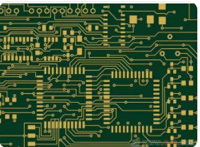
Creation of the middle layer
The Protel system provides a special layer setting and management tool-Layer Stack Manager (Layer Stack Manager). This tool can help designers add, modify and delete working layers, as well as define and modify layer attributes. Select [Design]/[Layer Stack Manager…] command to pop up the layer stack manager property setting dialog box.
There are 3 options that can be set in this dialog box.
(1) Name: Used to specify the name of the layer.
(2) Copper thickness: Specify the copper film thickness of this layer, the default value is 1.4mil. The thicker the copper film, the greater the current carrying capacity of a wire of the same width.
(3) Net name: Specify the network connected to this layer in the drop-down list. This option can only be used to set the internal electrical layer, the signal layer does not have this option. If the internal electrical layer has only one network such as "+5V", then the network name can be specified here; but if the internal electrical layer needs to be divided into several different areas, then do not specify the network name here.
There are insulating materials between the layers as the carrier of the circuit board or for electrical isolation. Among them, Core and Prepreg are both insulating materials, but Core has copper films and wires on both sides of the board, while Prepreg is only an insulating material used for interlayer isolation. The property setting dialog box of both is the same. Double-click Core or Prepreg, or select the insulation material and click the Properties button to pop up the insulation layer property setting dialog box.
The thickness of the insulating layer is related to factors such as interlayer withstand voltage and signal coupling, and has been introduced in the previous layer number selection and superposition principle. If there is no special requirement, the default value is generally selected.
In addition to the two insulating layers "Core" and "Prepreg", there are usually insulating layers on the top and bottom layers of the circuit board.
There is a stacking mode selection drop-down list under the options of the top and bottom insulation layer settings, and different stacking modes can be selected: Layer Pairs, Internal Layer Pairs and Build-up ). As mentioned earlier, the multilayer board is actually made by pressing multiple double-layer boards or single-layer boards. Choosing different modes means that different pressing methods are used in actual production, so "Core" and "Prepreg" The location is also different. For example, the layer pairing mode is two double-layer boards sandwiching an insulating layer (Prepreg), and the inner electric layer pairing mode is two single-layer boards sandwiching a double-layer board. The default Layer Pairs mode is usually used.
There is a list of layer operation buttons on the right side of the layer stack manager property setting dialog box. The functions of each button are as follows.
(1) Add Layer: Add an intermediate signal layer. For example, if you need to add a high-speed signal layer between GND and Power, you should select the GND layer first. Click the Add Layer button, and a signal layer will be added under the GND layer. The default name is MidLayer1, MidLayer2, ..., and so on. Double-click the name of the layer or click the Properties button to set the layer properties.
(2) Add Plane: Add internal electrical layer. The adding method is the same as adding the intermediate signal layer. First select the location of the internal electrical layer that needs to be added, and then click the button to add the internal electrical layer below the specified layer. The default names are Internal Plane1, InternalPlane2, ..., and so on. Double-click the name of the layer or click Properties The button can set the properties of the layer.
(3) Delete: delete a layer. Except for the top and bottom layers that cannot be deleted, other signal layers and inner electric layers can be deleted, but the middle signal layer that has been routed and the divided inner electric layer cannot be deleted. Select the layer to be deleted, click the button, a dialog box pops up, and click the Yes button to delete the layer.
(4) Move Up: Move up one layer. Select the layer that needs to be moved up (it can be a signal layer or an internal electric layer), click this button, and the layer will move up one layer, but it will not exceed the top layer.
(5) Move Down: Move down one layer. Similar to the Move Up button, click the button, the layer will move down one layer, but will not exceed the bottom layer.
(6) Properties: Properties button. Click this button to pop up the similar layer attribute setting dialog box.
After completing the relevant settings of the layer stack manager, click the OK button to exit the layer stack manager, and you can perform related operations in the PCB editing interface. When operating the middle layer, you need to first set whether the middle layer is displayed in the PCB editing interface. Select the [Design]/[Options...] command to pop up the option setting dialog box, and tick the internal electrical layer option under Internal planes to display the internal electrical layer.
After completing the settings, you can see the displayed layers under the PCB editing environment. Use the mouse to click the layer label of the circuit board to switch between different layers for operation. If you are not used to the default colors of the system, you can choose the Colors option under the [Tools]/[Preferences...] command to customize the colors of each layer. The related content has been introduced in Chapter 8 for readers' reference.