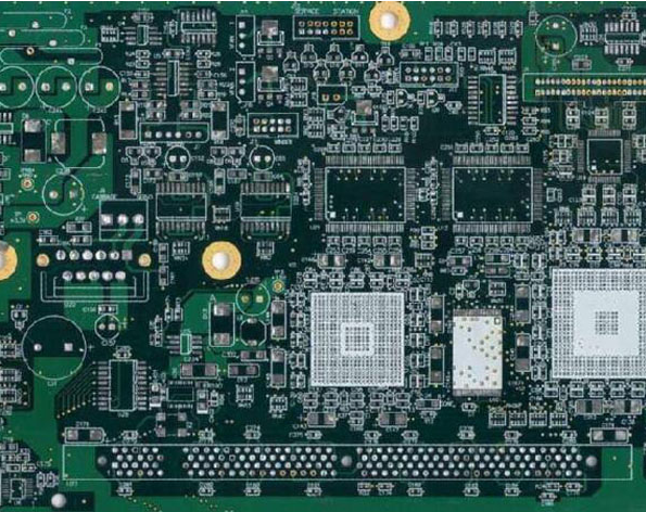
This article focuses on PCB designers who use IP, and further uses topology planning and routing tools to support IP to quickly complete the entire PCB design. As can be seen from Figure 1, the design engineer has the responsibility to obtain IP by arranging a small number of necessary components and planning the critical interconnection paths between these components.
Once the IP is obtained, the IP information can be provided to the PCB designer, and the PCB designer will complete the remaining design. PCB designers further use topology planning and routing tools to support IP to quickly complete the entire PCB design. Now there is no need to obtain the correct design intent through the interaction and iterative process between the design engineer and the PCB designer. The design engineer has obtained this information and the result is quite accurate, which is of great help to the PCB designer. In many designs, design engineers and PCB designers must perform interactive layout and routing, which may consume a lot of valuable time for both parties. From past experience, interactive operations are necessary, but time-consuming and inefficient.

The preliminary plan provided by the design engineer may only be a manual drawing, without proper component scale, bus width or pin output prompts.
As PCB designers participate in the design, engineers who use topology planning technology can obtain the layout and interconnection of certain components. This design may also require the layout of other components, the collection of other IO and bus structures, and the completion of all interconnections.
PCB designers need to adopt topology planning and interact with the PCB layout components under the layout to achieve the best layout and interactive planning, thereby improving the efficiency of PCB design. With the completion of the layout of key areas and high-density areas and the acquisition of topology planning, the layout may precede the final topology planning. Therefore, some topological paths may have to use the existing layout. Although they have a lower priority, they still need to be connected. Therefore, part of the planning revolves around the layout of the produced components.
In addition, this level of planning may require more detail to provide the necessary priority for other signals. Some obstacles before the automatic routing of a particular bus can provide the algorithm with options for other routing layers. Since the bus is organized into tight lines on the first layer, the designer begins to plan the conversion part as the third layer, with the details "3", and consider the distance the bus passes through the PCB. Note that this topology path on layer 3 is wider than the top layer because it requires extra space to accommodate the impedance. In addition, the design also specifies the exact location of the layer transition (17 holes). When the topological path moves down from the right part of Figure 3 to the detail "4", many single-bit T-shaped connection points need to be drawn from the topological path connection and each component pin. PCB designers choose to keep most of the connections on layer 3 and penetrate other layers to connect component pins.
Therefore, they drew a topological area to indicate the connection from the main harness to the fourth layer (pink), and connected the unit T-contact to the second layer, and then used other vias to connect to the device pins. The topological path continues at layer 3 to detailed information "5" to connect active devices. These connections are then connected from the active pins to the pull-down resistors under the active device.
The designer uses another topology area specification to connect from layer 3 to layer 1, where the component pins are active devices and pull-down resistors. This level of detailed planning can be completed in about 30 seconds. After obtaining this plan, PCB designers may wish to route immediately or create further topology planning, and then complete all topology planning through automatic routing. It takes less than 10 seconds from the completion of the plan to the result of the automatic wiring. In fact, this speed is not important. In fact, if you ignore the designer's intention, the quality of automatic routing is very poor, which is a complete waste of time. It takes about 10 seconds to perform high-quality automatic wiring. By raising the level of abstraction to topology planning, the entire interconnection time is greatly shortened. Before the interconnection starts, the designer has a truly clear understanding of the density and the potential to complete the design. For example, why keep the line at this point in the design? Why not continue planning and add lines at the back? When is the complete topology planned?
If you consider the above example, the plan abstraction can be used with another plan instead of 17 independent networks with many segments and many holes on each network. This concept is very important when considering engineering change orders (ecology, project) .
Engineering Change Order (ECO) In the following example, the FPGA pin output has not yet been completed. Design engineers have informed PCB designers of this reality, but for progress reasons, they need to advance the design as much as possible before the FPGA pin output is completed. In the case of known pin output, PCB designers begin to plan the FPGA space, and the designers complete the planning at the same time, while also considering leading from other devices to the FPGA. The IO was originally planned to be on the right side of the FPGA, but is now on the left side of the FPGA, causing the pin output to be completely different from the original plan.
PCB designers can use topology planning tools at the beginning of the design, or they can use them after the design engineer obtains the IP, depending on who uses this flexible tool to best adapt to their design environment. Topological wiring just follows the designer's plan or intention to provide high-quality PCB wiring results. When facing ECO, topology planning is much faster than a separate connection operation, so topology wiring equipment can adopt ECO more quickly, thereby providing fast and accurate results.