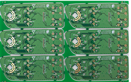
PCB design often has some errors during the import process of the schematic diagram. Next, I will introduce the common errors in the process of importing the schematic diagram-the package assignment does not exist or is incorrect, as well as the processing methods and techniques.
If there is a device in the schematic diagram that is not packaged, a warning message will pop up, indicating that the virtual component cannot be exported. In this case, no default packaging information will be imported into the layout, and the components will simply be deleted from the layout. If the package import has passed, but the valid package shape cannot be matched correctly, an alarm message indicating the mismatch will also be generated during the import process.
Correct the package assignment in the PCB schematic, or create a valid package for any device. After correction, perform the forward labeling step to update and synchronize the design information.
Update PCB design through annotation
Annotation is the process of importing PCB design changes from the schematic to the layout or from the layout to the schematic. Backward labeling (from layout to schematic) and forward labeling (from schematic to layout) are the keys to keeping the design accurate.
In order to protect the work that has been done, the current version of the schematic and layout files need to be backed up and archived before any important forward or backward annotation steps.

Don't try to make changes in the schematic and layout at the same time. Make changes to only a part of the schematic or layout of the PCB design, and then perform the correct marking steps to synchronize the design data.
Renumber the device
Device renumbering refers to a function of renumbering the components on the PCB in a specific order. The reference numbers should be sorted from top to bottom and from left to right on the PCB. This makes it easier to locate the device location on the board during assembly, testing, and troubleshooting.
Handle last-minute device or netlist changes
Last-minute PCB device or netlist changes are not desirable, but sometimes they have to be done because of device availability issues or detection of last-minute design errors. If you need to change the component or netlist, it should be done in the schematic, and then forward annotated to the layout tool.
Here are some PCB design tips:
If you add a new device (such as adding a pull-up resistor to the open-drain output) after the layout design starts, add resistors and networks to the design from the schematic. After being marked in the forward direction, the resistor will be displayed outside the circuit board frame as an un-layout component, and a flying line will be displayed to indicate the connection to the network. Next, move the components to the outer frame of the circuit board and perform normal wiring.
Backward labeling and reference number changes can work well together, such as renumbering the poster layout.
Select the positioning device by highlighting
In the PCB layout process, one way to browse specific components or traces in the schematic is to use the ‘highlight selection’ function. This function allows you to select a component or a trace (or multiple objects), and then view their position in the schematic.
This function is especially useful when matching bypass capacitors and their corresponding IC connections. Conversely, you can also locate specific PCB components or traces in the layout when browsing the schematic.