1., Inner line
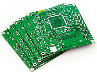
About PCB Circuit Board,copper foil substrate is first cut to the size suitable for processing and production. Before pressing the film on the substrate, the copper foil on the surface should be roughened properly using brushing, micro-etching, etc., and then the dry film photoresist is tightly attached to it at appropriate temperature and pressure. The substrate with good dry film photoresist is sent into the ultraviolet exposure machine, and the photoresist will produce a polymerization reaction after being irradiated by ultraviolet light in the transmittance area of the film, and the circuit image on the film is transferred to the dry film photoresist on the board. After the protective film on the film surface is torn off, the unilluminated area on the film surface is developed and removed by sodium carbonate aqueous solution, and the exposed copper foil is corroded and removed by hydrogen peroxide mixed solution to form the circuit. Finally, the successful dry film photoresist was washed away with light sodium oxide aqueous solution.
2, Pressing
After completion, the inner circuit board shall be bonded with the outer circuit copper foil by glass fiber resin film. Before pressing, the inner plate shall be treated with black (oxygen) to make the copper surface passivated and increase the insulation; The copper surface of the inner circuit is coarsened so that it can produce good bonding performance with the film. When stacking, the inner PCB circuit board above the six layers shall be riveted in pairs with a riveting machine. Then the plate is neatly stacked between the mirror plate and sent into the vacuum press to make the film harden and bond at appropriate temperature and pressure. After pressing the circuit board, the target hole drilled by an X-ray automatic positioning drilling machine is used as the reference hole for line alignment of inner and outer layers. And the plate edge to do the appropriate fine cutting, to facilitate subsequent processing.

3, Drilling
Drill the circuit board with a CNC drilling machine to drill the conducting hole of the interlayer circuit and the fixed hole of the welding parts. When drilling, the circuit board is fixed on the drilling machine table with the plug through the previously drilled target hole. At the same time, the flat bottom backing plate (phenolic resin board or wood pulp board) and the upper cover plate (aluminum plate) are added to reduce the occurrence of drilling burr.
4., Plated through the hole
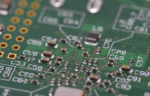
After the formation of the inter-layer through-hole, a copper layer shall be laid on it to complete the inter-layer circuit. First, the hair on the hole and the powder in the hole are cleared using heavy brush grinding and high-pressure washing, and the tin is immersed and attached to the cleaned hole wall.
Primary copper is a colloidal layer of palladium, which is then reduced to metal palladium. The circuit board is immersed in the chemical copper solution, and the copper ions in the solution are reduced and deposited on the hole wall by the catalytic action of palladium metal to form a through-hole circuit. Then the copper layer in the conductive hole is thickened by copper sulfate bath electroplating to be thick enough to resist the subsequent processing and use of environmental impact.
5., Secondary copper for outer line
The production of line image transfer is similar to that of the inner line, but it can be divided into two production modes of positive and negative film in line etching. The negative film production mode is like the inner line production, which is completed by etching copper directly and removing the film after development. The production method of the positive film is to add secondary copper and tin-lead plating after development (tin-lead in this area will be retained as an etching inhibitor in the later steps of copper etching). After removing the film, the exposed copper foil will be corroded and removed with alkaline ammonia water and copper chloride mixed solution to form a circuit. Finally, the tin-lead stripping liquid will be successful to remove the tin-lead layer (in the early had retained the tin-lead layer, after the heavy melting used to cover the line as a protective layer, now more than not).
6. , Anti-welding ink text printing
Earlier green paint is produced by direct heat drying (or ultraviolet radiation) after screen printing to harden the paint film. But because of its in the process of printing and hardening often cause green paint penetration into the copper surface of the line terminal contact and parts welding and use the trouble, now in addition to the simple and rough circuit board use, more sensitive green paint for production.
The text, trademark, or part label required by the customer is printed on the board in the way of screen printing, and then the text paint ink is hardened by hot drying (or ultraviolet radiation).
7. , Contact processing
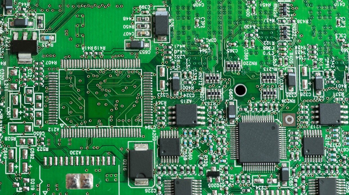
The anti-welding green paint covers most of the copper surface of the circuit, and only the terminal contacts for welding parts, electrical testing, and circuit board insertion are exposed. The endpoint should be added with an appropriate protective layer to avoid oxide generation at the endpoint connected with the anode (+) in long-term use, which will affect circuit stability and cause safety concerns.
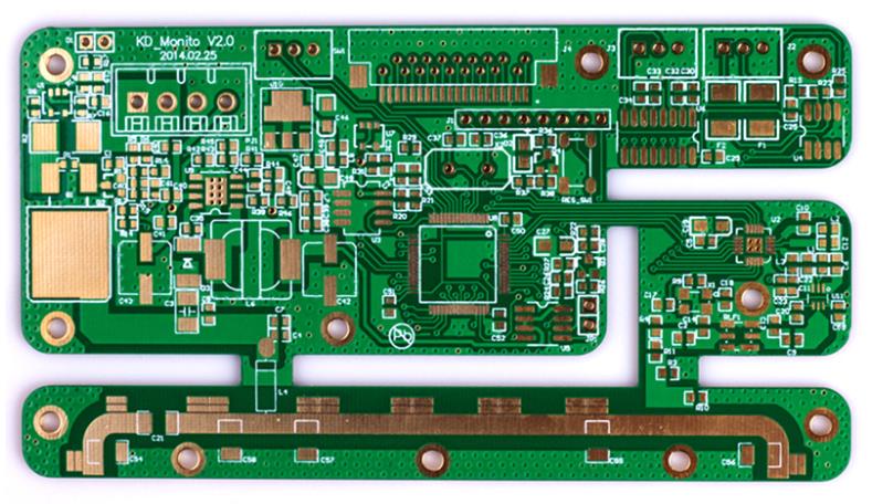
8., Molding cutting
The circuit board will be a CNC molding machine (or die punch) cut into the size of customer requirements. When cutting, the circuit board is fixed on the bed (or mold) with the plug through the positioning hole drilled previously. After cutting, gold finger parts are ground bevel machining to facilitate the use of circuit board insertion. For the multi-coupling-shaped circuit board, it is necessary to open the X-shaped broken line to facilitate the customer to divide and disassemble after the plug-in. Finally, the dust on thecircuit board and the ionic contaminants on the surface are washed.