Summarize 13 points of high-frequency circuit wiring skills
PCB factory: 1. The less the lead bends between the pins of the high-speed circuit device, the better. It is best to use a full straight line for the wiring of the high-frequency circuit, and it needs to be turned. It can be turned by a 45° broken line or a circular arc. Meeting this requirement can reduce the external emission and mutual coupling of high-frequency signals.
2. The shorter the lead between the pins of the high-frequency circuit device, the better.
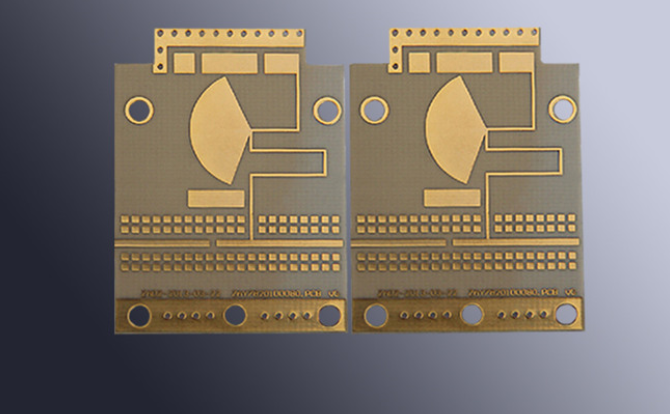
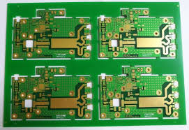
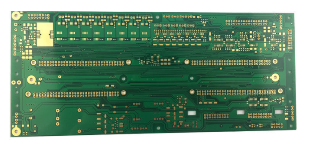
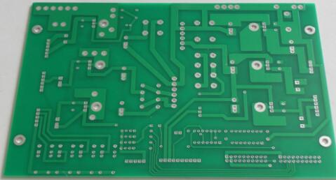
3. High-frequency circuits tend to have high integration and high wiring density. The use of multi-layer boards is not only necessary for wiring, but also an effective means to reduce interference.
4. Various signal traces cannot form loops, and ground wires cannot form current loops.
5. A high-frequency decoupling capacitor should be installed near each integrated circuit block.

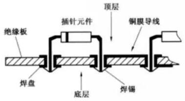
6. The fewer lead layers alternate between pins of high-frequency circuit devices, the better. The so-called "the less the inter-layer alternation of the leads, the better" refers to the vias used in the component connection process (Via, the less the better. According to measurements, one via can bring about 0.5 pF of distributed capacitance and reduce the number of vias. Can significantly increase the speed.
7. For high-frequency circuit wiring, attention should be paid to the "cross interference" introduced by the signal lines in close parallel routing. If parallel distribution cannot be avoided, a large area of "ground" can be arranged on the opposite side of the parallel signal lines to greatly reduce interference. Parallel wiring in the same layer is almost unavoidable, but in two adjacent layers, the direction of the wiring must be perpendicular to each other.
8. Implement ground wire enclosing measures for particularly important signal lines or local units, that is, draw the outer contour line of the selected object. Using this function, it is possible to automatically carry out the so-called "packing ground" processing on the selected important signal lines. Of course, using this function for the clock and other units to partially carry out the packet processing will also be very beneficial to the high-speed system.
9. Before DSP, off-chip program memory and data memory are connected to the power supply, filter capacitors should be added and placed as close as possible to the power supply pins of the chip to filter out power supply noise. In addition, shielding is recommended around key parts such as DSP and off-chip program memory and data memory to reduce external interference.
10. Use high-frequency choke links when connecting analog ground wires and digital ground wires to public ground wires. In the actual assembly of the high-frequency choke link, the high-frequency ferrite bead with a wire through the center hole is often used. It is generally not expressed in the circuit schematic diagram. The resulting netlist (netlist, not Including this type of component, it will ignore its existence when wiring. In view of this reality, it can be used as an inductor in the schematic diagram, and a component package can be defined separately for it in the PCB component library, and it can be manually moved to before wiring. At a suitable location close to the junction of the common ground.
11. The analog circuit and the digital circuit should be arranged separately, and the power and ground should be connected at a single point after independent wiring to avoid mutual interference.
12. The off-chip program memory and data memory should be placed as close to the DSP chip as possible, and at the same time, the layout should be reasonable so that the length of the data line and the address line are basically the same, especially when there are multiple memories in the system, the clock line to the clock of each memory should be considered The input distance is equal or a separate programmable clock drive chip can be added. For a DSP system, an external memory with an access speed similar to that of the DSP should be selected, otherwise the high-speed processing capability of the DSP will not be fully utilized. DSP instruction cycle is nanosecond level, so the most likely problem in DSP hardware system is high frequency interference. Therefore, when making the printed circuit board(PCB, etc.) of DSP hardware system, pay special attention to the important The wiring of the signal line should be correct and reasonable. When wiring, try to make the high-frequency line short and thick, and keep it away from the signal line that is susceptible to interference, such as analog signal line. When the circuit around the DSP is complicated, it is recommended to use the DSP and its clock The circuit, reset circuit, off-chip program memory, and data memory are made into the smallest system to reduce interference.
13. When following the above principles and proficient in the use of design tools, after manual wiring is completed, in order to improve the reliability and productivity of the system, high-frequency circuits generally need to be simulated by advanced PCB simulation software.