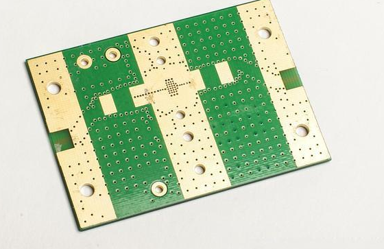
1, the weight of the circuit board itself will cause the board depression deformation
General welding furnace will use the chain to drive the circuit board in the welding furnace forward, that is, when the two sides of the board when the fulcrum to support the whole board, if the board above the overweight parts, or the size of the board is too large, because of the amount of its own and appear in the middle of the depression phenomenon, resulting in plate bending.

2. The depth of V-cut and the connecting strip will affect the deformation of the panel
Basically, V-cut is the culprit of destroying the sub-structure of the board, because V-cut is to Cut grooves on the original large sheet, so it is easy to deform the place of V-cut.
3. Deformation caused by PCB board processing
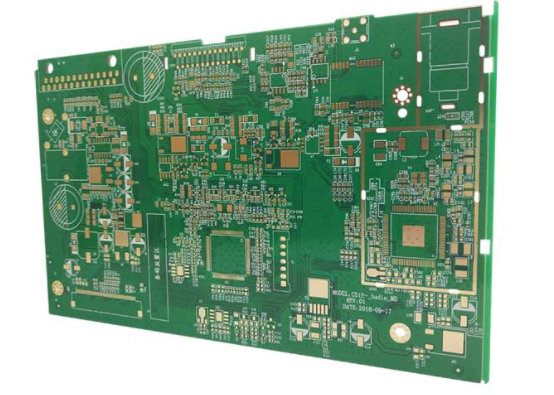
The cause of deformation of PCB board is very complex and can be divided into thermal stress and mechanical stress. The thermal stress mainly occurs in the process of pressing, while the mechanical stress mainly occurs in the process of stacking, handling and baking. The following is a brief discussion in order of flow.
Copper clad plate incoming material: copper clad plate are double panels, symmetrical structure, no graphics, copper foil and glass cloth CTE are almost the same, so in the process of pressing almost no deformation caused by different CTE. However, the large size of the copper clad plate press and the temperature difference in different areas of the hot plate will lead to slight differences in the curing speed and degree of the resin in different areas during the pressing process. At the same time, the dynamic viscosity under different heating rates is also greatly different, so it will also produce local stress caused by the difference in the curing process. Generally, this stress will maintain balance after pressing, but will gradually release deformation in the future processing.
Pressing: PCB pressing process is the main process to produce thermal stress, and the deformation caused by different materials or structures is analyzed in the previous section. Similar to copper-clad plate compression, local stress caused by the difference in curing process can also be generated. PCB board due to thicker thickness, diversified pattern distribution, more semi-cured pieces, etc., its thermal stress will be more difficult to eliminate than copper-clad plate. The stress in PCB board is released in subsequent drilling, shaping or barbecuing processes, resulting in deformation of board parts.
Resistance welding, character and other baking process: because the resistance welding ink curing can not stack each other, so PCB board will be placed in the shelf drying board curing, resistance welding temperature is about 150 degree Celsius, just over the Tg point of the medium and low Tg material, the resin above the Tg point is high elastic, the board is easy to deformation under the action of dead weight or oven strong wind.
Hot air solder leveling: ordinary plate hot air solder leveling tin furnace temperature is 225 degree Celsius~265 degree Celsius, time is 3s-6s. The hot air temperature is 280 degree Celsius~300 degree Celsius. Solder plate from room temperature into the tin oven, out of the oven within two minutes after the room temperature post-processing washing. The whole hot air solder leveling process is sudden heat and cold process. Because the circuit board material is different, the structure is not uniform, in the process of hot and cold will inevitably appear thermal stress, resulting in microscopic strain and overall deformation warping zone.
Storage: The storage of PCB board in the semi-finished stage is generally firmly inserted in the shelf, the improper adjustment of the shelf, or stacking the board in the storage process will cause mechanical deformation of the board. Especially for 2.0mm or less thin plate impact is more serious.