Interconnect technology of encapsulation chips with high performance and reliability-IC Packaging
The market development direction of electronic components(For Printed Circuits Board Assembly-PCBA)
For the mature technology of LSI with higher integration and speed, it is necessary to develop isolation technology using low K materials as appropriate. But in order to satisfy the high performance of these units, the isolation becomes thinner and thinner because of the porous and multilayer structure. As a result, LSI becomes brittle. On the other hand, in order to meet the high-speed requirements, the current of LSI is constantly increased. In addition to the chip size from large to small, thermal density and power consumption are also increasing. Therefore, for the semiconductor packaging substrate(IC Substrate Packaging) in the future, it is required to solve these problems, namely, the fragility of the interlayer media, high heat, high speed and low cost. The future presupposition of semiconductor processes will be in the 20nm generation and below, which will be much weaker.
Packaging technology required for 20nm generation
The specification required for the next generation of 20nm is:
Low stress for brittle low K layer
High thermal radiation ≥5W for high-performance LSI
High speed ≥10GHz for high functionality
Semiconductor packaging development direction
In order to accommodate the functional growth and cost reduction of electrical facilities including mobile facilities, wafer preset rules are moving towards larger and finer preset rules. To this end and to reduce costs, semiconductor packaging technology is rapidly shifting from the most standard bonding technology of gold wire bonding to copper wire bonding, which reduces the amount of gold used. In addition, the use of flip-chip bonding technology has greatly satisfied LSI's higher integration and performance. In 2010, flip-chip bonding accounted for 15 percent and lead bonding 85 percent of the world's semiconductor packaging technology. By 2015, the share of flip-chip bonding is expected to reach 25 percent, and the share of lead bonding is expected to reach 75 percent. Especially for high integration and high-performance LSI which requires high thermal radiation and high signal speed, flip-chip bonding technology is being actively considered as appropriate.
Common sense flip-chip technology
Suitability for low K
Commonly used flip chip technology:
. Welding adjacent flank, the main structure is C4 (controllable subsidence chip co-sign)
. For pressure bonding of Au bump and ACF type
. Ultrasonic bonding for AU-AU type signature
Pressure and ultrasonic bonding have high pressure and mechanical oscillation applied to LSI, so these methods cannot be used for low K LSI. Because of this, in the above method, C4 can be used as appropriate, and because of the comparison of the three methods, the bond is consistent with the fact that C4 does the least damage to the chip.
C4 technology was created in the early 40s for general-purpose computers and has been in use ever since. With the increasing number of low K wafers, C4 was used for low K by replacing UBM structures, materials and improvements.
Recently developed Cu column bumps (roughly similar to advances in C4) are suitable for in-line or overlapping pads, not for low K wafers. It has been reported that Cu column structure encapsulation may damage the low k layer due to the high elastic modulus of Cu (130GPa). The mismatch of thermal expansion coefficient (CTE) is the acceleration factor.
In addition, the C4 technology originally used molten metal junction after the flux and the high elastic modulus of the flux (50GPa) deemed appropriate, so the amount of stress was added to LSI due to the difference in heating expansion during bonding and installation of the mother plate. Therefore, C4 technology cannot be used for future LSI, which is much weaker.
Thermal radiation
Until now, organic substrates have been used for flip-chip packaging. The thermal conductivity of organic substrates is small, 0.5 W/ MK, and it is difficult to apply to LSI with high power consumption. If a cooling or cooling system is added to improve thermal radiation, the cost of encapsulation, the size and height of the plane or surface will increase.
In fact, because the heat radiation is low, a bit of LSI limits its potential so as not to generate a large amount of heat. In addition, because the heat radiation is not good, the junction temperature increases, the leakage current increases, which further increases the power consumption, and the increase in power consumption makes the temperature rise. It is a dangerous vicious circle. Therefore, the improvement of thermal radiation is a close problem.
High speed of the signal
The medium damage loss of the central layer of the organic substrate is high (0.02), and the impedance of the through hole (T/H) of the central layer is high. As a result, the insertion damage loss in the high frequency range is high. However, using coreless substrates of the same material as traditional organic substrates is not the fundamental solution. In addition, composite layer materials can be a variety of, so the user to choose the best material is more difficult, the whole preset requirements to think about the problem of high speed performance.
Because the substrate is thin, a series of facilities need to be changed. This becomes a stumbling block to production. Because of this problem, transferring to a coreless substrate is high-risk and only suitable for localized products.
Traditional technology is difficult to satisfy the future 20nm generation. Therefore, it is necessary to develop new semiconductor packaging with new central technology.
Monsterpac-typec and process essentials
Monsterpac-typec was developed to satisfy the 20nm process, which is difficult to fit with traditional packaging technology. This is the traditional packaging process and structure is absolutely different from the packaging.
Encapsulation structure
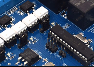
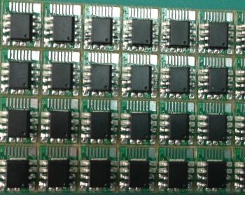
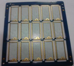
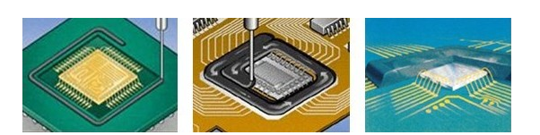
Our packaging structure, the substrate is ceramic, semiconductor chip with bump flip, chip and substrate supplement NCP (non-conductive paste). It is not moulded with epoxy gas or natural resin. So the back of the chip is exposed. The high temperature warpage of reflow welding is small, less than 30-50μm, so the package is LGA(contact array package) without welding balls, not BGA(grid array package). A silver-containing conductive paste is used for bumps, which are printed on the substrate so that modules are no longer manufactured on the pads. Non-plating nickel and gold only on the Al pads of the chip without the wafer bump process (Figure 1-3).

FIC-1 Packaging Structure

FIC-2 Packaging Image

FIC-3 Process
Broadly similar to the above, our package consists of only 4 materials (chip, bump, ceramic and NCP). This simple structure makes for a small, thin and lightweight package.
There are two main types of ceramic substrate materials available: HTCC (high temperature co-fired ceramic) and LTCC (low temperature co-fired ceramic). The special properties of ceramics (such as electrical properties, temperature conductivity, CTE and warping) and flip chip bonding enable our packages to satisfy the best solution for a wide range of requirements from electrical products to semiconductor chips.
Monsterpac-typec structure is unique
The unique places are described as follows:
. No damage bonding
. High thermal radiation
. Low insertion loss
. High reliability
By combining each of these major advantages, the MonsterPac-TypeC succeeds in delivering the best possible performance for the 20nm generation LSI.
No damage bond
The core technology of our package is the no-damage flip-chip bonding technology, which successfully achieves no-damage and highly reliable bonding for semiconductor chips manufactured with cutting-edge precision processing.
Semiconductor chips without damage refers to:
Low pressure bonding
We can achieve a bonding pressure of 0.12g/ bump, which is 1/20 of the normal C4's 2.4g/ bump. By reducing the bonding load to this limit, damage of the bonding induced interlaminar medium can be avoided.
Low retraction stress during convex curing
The shrinkage stress during the solidification of the convex point is less than 10MPA/ convex point, which is very small. High yield and reliable flip-chip bonding is successfully achieved by upper limit reduction of temperature, load and retracting stress applied to the middle layer of the brittle medium (such as low K and Al pads and lines, etc.) to avoid line breakage and cracks.
From these advantages, it can be seen that it is the only package with the structure to avoid weak low K layer damage.
High thermal radiation
Realizing that the calories of the semiconductor chip are radiated by the encapsulated substrate, instead of the common organic substrate (thermal conductivity of 0.5W/mk), we chose the ceramic substrate, because its thermal conductivity is more than the organic substrate, which is 14W/mk. When the package size is 21*21mm and the ceramic substrate is used, the power dissipation reaches 6W, which is 1.7 times higher than that of the organic substrate with 3.6W power dissipation.
A low insertion will hurt you
Electronic facilities require high level performance in the high frequency range. The insertion loss of ceramic substrate is 0.42dB (@20GHz, L=5mm), while that of organic substrate is 0.62dB. The frequency allowed by ceramic substrate is more than 10GHz, while that of organic substrate is 3GHz.
High reliability and high tolerance to moisture resistance
Normal reflow resistance (MSL: Wetness Level) is Level 3 (@30DEG /60 100% RH192Hr). Monsterpac-typec each has one semiconductor chip that is undamaged and the bumps are made of non-fused material. At high temperature reflow, the bump is not fused, so it does not repeat re-melting and re-curing, and the ceramic substrate does not borrow moisture. As a result, the MonsterPac-TypeC is MSL Level 1 (@85DEG /85 100% RH192Hr), it does not have to be pre-baked to remove moisture and moisture proof packaging, and the plant life of the MonsterPac-TypeC is unlimited.
High plant rate
Instead of welding bumps, we developed an epoxy gas bump structure to facilitate production. As a result, a large number of wafer bump process facilities are necessary, the cost of a large number of can + wisp welding adjacent to reflow is also necessary. So, compared to a conventional C4 process plant of the same size, the size of the plane or surface of the plant can be reduced by 69 percent, and the energy consumption of the plant can be reduced by 85 percent. Can successfully achieve energy saving and low background load plant.

Capacity
Monsterpac-typec process unique place
Ceramic technology bump
Monsterpac-typec sees fit to use a silver-containing conductive paste as the bump material. To form bumps on the ceramic substrate using the usual weld-printing SMD parts printing technique as deemed appropriate. There is no need to pre-dispose and clean the surface of ceramic substrate before raising point disposal and to electroplate the surface after raising point formation. Conventional organic FCBGA requires long bumps, such as flux, Au and Cu bumps, on the Al pads of semiconductor wafers. However, ceramic based bumps do not require this wafer long bump process. Instead, they produce non-electroplated Ni and Au on semiconductor chips. The bumps based on ceramic technology have successfully realized the process of simple disposal and low cost.
In addition, unlike the hard bumps (hardness ≥10Hv) used in common sense techniques such as flux, Au and Cu bumps, soft bumps (≤1Hv) have been developed to maintain the pattern under low hardness.
For silver-containing soft convex conductive pastes, we have developed concerned fixation points that are experienced in low stress, low countersign resistance and detail pitch printing. The labor capacity we have so far formed bumps is face array pads: pitch 150μm; Peripheral pads: Pitch 75μm. However, this pad pitch is considered by the actual preset rule, so the surface array pitch of 60μm is applicable for only opening bumps.
No damage bond
With the soft flip chip bonding technology, the NCP used to distribute the soft bumps formed by the ceramic bump technology, and then the semiconductor chip is bonded with the flip chip. During the bonding process, the conductive paste of the bumps and the NCP are solidified at the same time. As a result, both cosignature and dependability are achieved successfully.
The temperature of the FCB facility is below 200 degree Celsius, which is more than 40 degree Celsius lower than the normal bonding technology. The bonding pressure is less than 0.12g/ dot, which is 1/20 of the normal bonding technology. With these low temperature and low pressure hot pressing bonds, semiconductor chips are not subjected to stress and external forces during bonding and post-bonding curing. Using the newly developed conductive paste and NCP, the high-speed key timing below 1.0 seconds was successfully achieved. The NCP includes supplements, which are commonly found on both sides of the chip pad and the bump. However, it is common to flip the chip keys at low pressure. The supplement is buried in the bumps, so it does not affect the signature between the chip pad and the bumps. This is one of the advantages of soft bumps. After the distribution of NCP before the flip chip welding, NCP is easily supplemented between the convex point and narrow gap, and with the low load key, the aiming between the chip and the substrate will not occur. Therefore, this bonding technique is suitable for use with narrow pad pitches.
The problem with common bonding techniques is that in the case of flip-chip bonding with weld bumps, very large retract stresses (about 200-500 mpa/bump) are applied to the bumps and Al pads of the semiconductor chip during flux melting to curing. However, the low stress bonding technique is successful because the low elastic modulus of non-molten convex materials requires a very small rebounding stress (less than 10MPa/ convex).
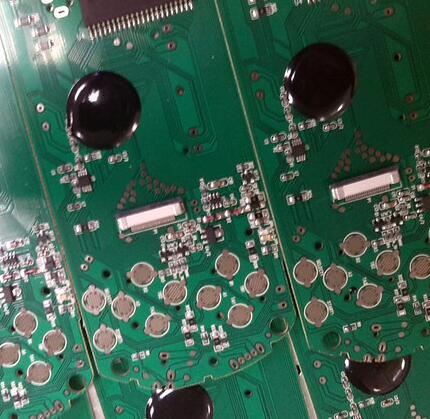
Because of the above mentioned process of these basic technology development, the success of the undamaged flip chip bonding. FIG. 4 is a cutaway view of the flip chip's keypoint and countersign.

FIG-4 Visual and Section Photo

Packaging Reliability
TC tested the profile of the rear convex point, but did not test and measure the cracks and descaling that would be induced by fracture coupling.

APIC (Application device IC)
Today's APIC processing is moving towards the use of low-K materials for precision machining, which requires high temperature tolerance and high speed. The Monsterpac-TypeC satisfies these requirements with the advantages listed below.
. No damage bonding
. High thermal radiation
When high speed
A few APIC customers are evaluating the MonsterPAC-TypeC for scale production

PAC-TypeC
As a result of the actual evaluation between the organic FCBGA and monsterpac-TypeC under the same conditions (same skirt, same chip and same pad pitch), the monsterpac-TypeC temperature Tj is 10 degree Celsius lower than that of the organic package. After a very accurate comparison of Tj, the difference would be about 20 degree Celsius.
The RF Board(Radio Frequency Board):
At present, for high speed communication LSI, the plate encapsulation is constantly improving. These sections require special properties listed below:
. Suitable for high speed and high frequency
Low size small
For high speed and high frequency applications, as above, if appropriate, the use of ceramic substrate can improve the insertion loss, can be used for 10GHz.
In addition, multi-chip and high number of SMD parts can be used in small packages because of the availability of small, detail-pitch flip-chip bonding.
Cooperated with a customer of RF plate, developed a sample, its performance has been approved by the customer, is preparing for scale production

RF Module
For these plate enclosures, the wetness of the substrate is very tight. The MSL of monsterpac-TypeC is Level 1, so there is no wetting degree choking.
It can be seen that monsterPAC-TypeC is the most suitable for plate packaging, which requires multiple reflow welding for conventional organic packaging SMD and flip-chip.
Judge
For the coming generation of 20nm processes, packages are required to accommodate higher thermal radiation and higher speeds. However, common sense packaging technology is difficult to meet these requirements. Therefore, it is necessary to develop a new packaging technology suitable for the 20nm process generation.
Our Monsterpac-TypeC is suitable for the upcoming 20nm process generation and maximizes LSI performance. Its high performance is like an amazing weird product. MonsterPAC, which we developed, made C4 obsolete and became the main technology contributing to the next generation of semiconductors in the future.
For the next generation of technology development
Research and development of new ceramic substrate
The development of ceramic substrate technology has been more than bright. Up to now, precise and detailed plotting with high density has lagged far behind organic IC Substrates.
In order to solve this problem and make progress, we set out to develop a precise ceramic substrate with high density without affecting the cost. Our goal is 20μm line pitch, to achieve as appropriate and the use of precision and detailed graphics more flexible default, through hole pitch also needs to be more precise and detailed, the goal is 50μm.
Up to now the ceramic substrate has been made using punch and mask printing as deemed appropriate. These existing techniques are very limited to precise and detailed drawing. We are thinking of replacing them with laser and direct printing processes. Implementing this technology will provide much better performance than organic substrates. Until now, ceramic substrates have been commonly used in high-end products, however, this new substrate will be aimed at consumer products. And the substrate really needs high performance consumer products to grow itself.
The combination of this substrate and MonsterPAC technology will provide the world with the best performance and high reliability Printed Circuits Board(PCB).