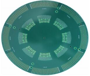
[IC Substrate manufacturer] the whole process from IC chip design, manufacturing to packaging
1, Complicated IC chip design process
The process of chip manufacturing is like building a house with LEGO. After the wafer is used as the foundation, and then the chip manufacturing process is stacked up layer by layer, the necessary IC chips can be produced (these will be introduced later). However, without design drawings, it is useless to have strong manufacturing capacity. Therefore, the role of architects is very important. But who is the architect in IC design? Next, this paper will introduce the IC design.
In the IC production process, most ICs are planned and designed by professional IC design companies, such as MediaTek, Qualcomm, Intel and other well-known manufacturers, all design their own IC chips and provide chips with different specifications and efficiency for downstream manufacturers to choose. Because IC is designed by each factory, IC design depends on the technology of engineers, and the quality of engineers affects the value of an enterprise. However, when engineers design an IC chip, what are the steps? The design process can be simply divided into the following.

IC Manufacture Process
Design the First Step and Set Goals
In IC design, the most important step is specification. This step is like deciding how many rooms and bathrooms are required before designing the building, what building regulations need to be complied with, and designing after determining all functions, so as not to spend additional time on subsequent modifications. IC design also needs to go through similar steps to ensure that the designed chip will not have any errors.
The first step in specification formulation is to determine the purpose and efficiency of IC and set the general direction. The next step is to see which protocols to comply with. For example, the chip of the wireless network card needs to comply with IEEE 802.11 and other specifications. Otherwise, the chip will not be compatible with the products on the market, making it unable to connect with other devices. The last is to establish the implementation method of the IC, allocate different functions into different units, and establish the connection method between different units, so as to complete the formulation of specifications.
After designing the specifications, the details of designing the chip are followed. This step is like writing down the architectural plan initially and drawing out the overall outline for the convenience of subsequent drawing. In IC chip, hardware description language (HDL) is used to describe the circuit. The commonly used HDL includes Verilog, VHDL, etc. the function of an IC can be easily expressed by code. Then check the correctness of the program function and continue to modify it until it meets the desired function.

Verilog example of 32 bits adder
With computers, everything becomes Easy
With a complete plan, the next step is to draw a board design blueprint. In IC design, the step of logic synthesis is to put the determined HDL code into the electronic design automation tool (EDA tool), and let the computer convert the HDL code into logic circuit to produce the following circuit diagram. Then, repeatedly determine whether the logic gate design drawing meets the specifications and modify it until the function is correct.

Results of control unit synthesis
Finally, put the synthesized code into another set of EDA tools for circuit layout and place and route. After continuous detection, the following circuit diagram will be formed. In the picture, you can see different colors such as blue, red, green and yellow. Each different color represents a light mask. As for how to use the mask?

layout and winding
Layers of masks, stacked a chip
First of all, it is known that an IC will produce multiple masks. These masks have upper and lower layers, and each layer has its own task. The following figure is a simple mask example. Taking CMOS, the most basic element in integrated circuits, as an example, the full name of CMOS is complementary metal oxide semiconductor, that is, combining NMOS and PMOS to form CMOS. As for what is metal oxide semiconductor (MOS)? This kind of component widely used in the chip is difficult to explain, and it is difficult for ordinary readers to understand. I won't study it more here.
In the figure below, the left side is the circuit diagram formed after circuit layout and winding. It has been known that each color represents a mask. On the right is the spread of each hood. Manufacturing is to start from the bottom, follow the method proposed in the previous article on the manufacturing of IC chips, make them layer by layer, and finally produce the desired chip.

So far, we should have a preliminary understanding of IC design. On the whole, it is clear that IC design is a very complex specialty. Thanks to the maturity of computer-aided software, IC design can be accelerated. The IC design factory relies heavily on the wisdom of engineers. Each step described here has its own expertise and can be independently divided into multiple professional courses. For example, writing hardware description language is not simple. It only needs to be familiar with the programming language, but also needs to understand how the logic circuit operates and how to convert the required algorithms into programs How synthetic software converts programs into logic gates.
2, What is a wafer?
In the news of semiconductors, we always mention wafer factories marked by size, such as 8-inch or 12-inch wafer factories. However, what is the so-called wafer? Which part is 8 inches? How difficult is it to produce large-size wafers? The following is a step-by-step introduction to the most important foundation of Semiconductors - what is "wafer".
Wafers are the basis for manufacturing all kinds of computer chips. We can compare chip manufacturing to building a house with Lego blocks, and complete our desired shape (that is, all kinds of chips) by stacking layer after layer. However, if there is no good foundation, the built house will be crooked, which is not what you want. In order to make a perfect house, you need a stable base plate. For chip manufacturing, this substrate is the wafer to be described next.

First of all, let's recall that when we played with high-rise blocks as children, there would be a small circular projection on the surface of the blocks. With this structure, we can stably stack the two blocks together without using glue. Chip manufacturing also fixes the subsequently added atoms and the substrate together in a similar way. Therefore, we need to find a substrate with neat surface to meet the conditions required for subsequent manufacturing.
In solid materials, there is a special crystal structure - single crystal. It has the characteristic that atoms are closely arranged one by one, and can form a flat atomic surface. Therefore, the above requirements can be met by using single crystal to make wafers. However, how to produce such a material? There are two main steps: purification and crystal drawing, and then such a material can be completed.
How to make a single crystal wafer
The purification is divided into two stages. The first step is metallurgical purification. This process is mainly to add carbon and convert silicon oxide into silicon with purity of more than 98% by means of oxidation-reduction. Most metal refining, such as iron or copper, uses this method to obtain metal of sufficient purity. However, 98% is still not enough for chip manufacturing and needs to be further improved. Therefore, Siemens process will be further used for purification. In this way, high-purity polysilicon required by semiconductor process will be obtained.

Silicon column manufacturing process
The next step is crystal drawing. First, the high-purity polysilicon obtained above is melted to form liquid silicon. Then, contact the liquid surface with a single crystal seed and slowly pull it up while rotating. As for why single crystal silicon is needed, it is because the arrangement of silicon atoms is the same as that of people in line. It will need a leader to let later people know how to arrange correctly. Silicon seeds are an important leader to let later atoms know how to queue. Finally, after the silicon atoms leaving the liquid surface solidify, the neatly arranged monocrystalline silicon columns are completed

Monocrystalline silicon column
However, what do 8 inches and 12 inches represent? He refers to the diameter of the crystal column produced by us, which looks like the part of the pencil holder. The surface is treated and cut into thin round pieces. What is the difficulty of making large-size wafers?
As mentioned above, the manufacturing process of crystal column is like making cotton candy, rotating and forming at the same time. If you have ever made marshmallows, you should know that it is very difficult to make large and solid marshmallows, and the process of crystal drawing is the same. The speed of rotation and temperature control will affect the quality of crystal column. Therefore, the larger the size, the higher the requirements for speed and temperature. Therefore, it is more difficult to make high-quality 12 inch wafers than 8-inch wafers.
However, a whole silicon column can not be made into a substrate for chip manufacturing. In order to produce silicon wafers one by one, it is necessary to cut the silicon column horizontally into wafers with a diamond knife, and then the wafers can be polished to form the silicon wafers required for chip manufacturing. After so many steps, the manufacturing of chip substrate is completed. The next step is to stack houses, that is, chip manufacturing. As for how to make chips?
Layers of stacked chips
After introducing what silicon wafers are, I also know that manufacturing IC chips is like building a house with Lego blocks, creating the desired shape by stacking layer after layer. However, there are quite a few steps to build a house, and so are IC manufacturing. What are the steps to manufacture IC? This paper will introduce the process of IC chip manufacturing.
Before we begin, we should first understand what IC chip is. IC, the full name of integrated circuit, can be seen from its name that it combines the designed circuits in a stacked manner. With this method, we can reduce the area required to connect the circuit. The following figure is a 3D diagram of IC circuit. It can be seen that its structure is like beams and columns of a house, stacked layer by layer, which is why IC manufacturing is compared to building a house.

3D profile of IC chip
From the 3D profile of IC chip in the figure above, the dark blue part at the bottom is the wafer introduced in the previous article. From this figure, we can know more clearly how important the wafer substrate plays in the chip. As for the red and khaki parts, they are to be completed during IC production.
First of all, the red part can be compared to the hall on the first floor of a high-rise building. The hall on the first floor is the gateway of a house. It is where people go in and out. It usually has more functionality under the control of traffic. Therefore, compared with other floors, the construction will be more complex and require more steps. In the IC circuit, this hall is the logic gate layer, which is the most important part of the whole IC. A variety of logic gates are combined to complete the IC chip with complete functions.
The yellow part is like a general floor. Compared with the first floor, it will not have too complex structure, and each floor will not change much during construction. The purpose of this layer is to connect the logic gates in the red part together. The reason why so many layers are needed is that there are too many lines to be connected together. When a single layer cannot accommodate all lines, it is necessary to stack several layers to achieve this goal. In this process, the lines of different layers will be connected up and down to meet the wiring requirements.
Layered construction and layer by layer structure
After knowing the structure of IC, we will introduce how to make it. Imagine that if we want to make a fine drawing with a paint spray can, we need to cut out the cover plate of the figure and cover it on the paper. Then spray the paint evenly on the paper. After the paint is dry, remove the shutter. After repeating this step, neat and complex graphics can be completed. Manufacturing IC is to stack layer by layer by covering in a similar way.
When making IC, it can be simply divided into the above four steps. Although the manufacturing steps and materials used are different in actual manufacturing, similar principles are generally adopted. This process is a little different from paint painting. IC manufacturing is first coated and then covered, while paint painting is first covered and then painted. Each process is described below.
-Metal splashing: evenly sprinkle the metal material to be used on the wafer to form a thin film.
-Coating photoresist: first place the photoresist material on the wafer, pass through the mask (the principle of the mask will be explained next time), hit the beam on the unwanted part, and destroy the structure of the photoresist material. Then, the damaged materials are washed away with chemicals.
-Etching technology: the silicon wafer without photoresist protection is etched by ion beam.
-Photoresist removal: dissolve the remaining photoresist using the photoresist removal solution, so as to complete a process.
Finally, many IC chips will be completed on a whole wafer. Next, as long as the completed square IC chips are cut off, they can be sent to the packaging factory for packaging. What is the packaging factory? I'll explain later.

Comparison of wafers of various sizes
3, What is the nanofabrication process?
Samsung and TSMC are very hot in the advanced semiconductor manufacturing process. They both want to take the lead in wafer foundry to win orders. It has almost become a dispute between 14nm and 16nm. However, what is the meaning of the two numbers of 14nm and 16nm, and which part does it refer to? What benefits and problems will it bring in the future after reducing the process? We will briefly explain the nano process below.
How subtle is Nano?
Before we start, we should first understand what nano means. Mathematically, the nanometer is 0.000000001 meters, but this is a very poor example. After all, we can only see many zeros after the decimal point, but we don't have a practical feeling. If the nail thickness is compared, it may be more obvious.
If you actually measure with a ruler and gauge, you can know that the thickness of the nail is about 0.0001 meter (0.1 mm), that is, try to cut the side of a nail into 100000 lines, and each line is about equivalent to 1 nm. Therefore, you can imagine how small 1 nm is.
After knowing how small nano is, we should also understand the intention of reducing the process. The main purpose of reducing transistors is to insert more transistors into smaller chips, so that the chips will not become larger due to technological improvement; Secondly, it can increase the operation efficiency of the processor; Moreover, reducing the volume can also reduce the power consumption; Finally, after the size of the chip is reduced, it is easier to plug it into the mobile device to meet the needs of lightweight in the future.
Then come back to explore what the nano process is. Take 14 nm as an example. The process refers to that the smallest wire in the chip can be 14 nm. The following figure shows the appearance of traditional transistors as an example. The main purpose of reducing the transistor is to reduce power consumption, but which part should be reduced to achieve this purpose?
The L in the lower left figure is the part we expect to shrink. By reducing the gate length, the current can use a shorter path from the drain end to the source end (if you are interested, you can use Google to search for MOSFET, which will be explained in more detail).

In addition, computers operate on 0 and 1. How can transistors meet this purpose? The method is to judge whether the transistor has current flow. When voltage is supplied at the gate terminal (Green Square), the current will flow from the drain terminal to the source terminal. If no voltage is supplied, the current will not flow, so it can represent 1 and 0( As for why we use 0 and 1 for judgment, if you are interested, you can check brin algebra. We use this method to make computers.)
Size reduction has its physical limitations
However, the manufacturing process cannot be reduced indefinitely. When we reduce the transistor to about 20 nm, we will encounter problems in quantum physics, so that the transistor has leakage, offsetting the benefits obtained when l is reduced. As an improvement method, the concept of FinFET (tri gate) is introduced, as shown in the upper right figure. In the previous explanation made by Intel, it can be known that the introduction of this technology can reduce the leakage caused by physical phenomena.

More importantly, this method can increase the contact area between the gate end and the lower layer. In the traditional practice (above left), the contact surface has only one plane, but after using FinFET (tri gate) technology, the contact surface will become three-dimensional, which can easily increase the contact area. In this way, the source drain end can be made smaller while maintaining the same contact area, which is very helpful to reduce the size.
Finally, it is why some people say that major factories will face quite severe challenges when entering the 10 nm process. The main reason is that the size of an atom is about 0.1 nm. In the case of 10 nm, there are only less than 100 atoms in a line, which is quite difficult to manufacture, and as long as there is a defect of one atom, such as atoms falling out or impurities in the manufacturing process, There will be an unknown phenomenon, which will affect the yield of the product.
If you can't imagine the difficulty, you can do a small experiment. Line up a 10 with 100 beads on the table * 10 square, and cut a piece of paper to cover the beads, then brush off the next beads with a small brush, and finally make him form a 10 * A rectangle of 5. In this way, we can know the difficulties faced by major factories and how difficult it is to achieve this goal.
As Samsung and TSMC will complete the mass production of 14 nm and 16 nm FinFET in the near future, they both want to compete for the OEM of Apple's next-generation iPhone chip. We will see quite wonderful commercial competition and obtain more power-saving and lightweight mobile phones. Thanks to the benefits brought by Moore's law.
4, Tell you what encapsulation is
Packaging, final protection and integration of IC chip
After a long process, from design to manufacturing, we finally got an IC chip. However, a chip is quite small and thin. If it is not protected outside, it will be easily scratched and damaged. In addition, because the size of the chip is small, it will not be easy to manually place it on the circuit board without a larger shell. Therefore, this paper will describe and introduce the packaging next.
At present, there are two common packages, one is the dip package common in electric toys, which looks like a centipede in black, and the other is the BGA package common when buying boxed CPU. As for other packaging methods, PGA (pin grid array) used by early CPUs; Pin grid array) or improved QFP (plastic square flatpack) of dip. Because there are so many packaging methods, dip and BGA packaging will be introduced below.
Traditional packaging, lasting
The first thing to introduce is the dual inline package; Dip), as can be seen from the figure below, the IC chip with this package will look like a black centipede at the foot of double row connection, which is impressive. This packaging method is the earliest IC packaging technology, which has the advantage of low cost and is suitable for small chips without too many wires. However, because most of them are plastic, the heat dissipation effect is poor, which can not meet the requirements of current high-speed chips. Therefore, most of the chips using this package are enduring chips, such as op741 in the figure below, or IC chips with less requirements for operation speed, smaller chips and fewer connection holes.

Amplifier cross-sectional view
As for ball grid array (BGA) packaging, compared with dip, the packaging volume is smaller and can be easily put into smaller devices. In addition, because the pin is located below the chip, it can accommodate more metal pins than dip, which is quite suitable for chips requiring more contacts. However, this packaging method has high cost and complex connection method, so it is mostly used in products with high unit price.

The schematic diagram of BGA using flip chip packaging
With the rise of mobile devices, new technologies have leapt onto the stage
However, using these packaging methods will consume a considerable volume. For example, mobile devices and wearable devices now require quite a variety of components. If each component is encapsulated independently, it will consume a lot of space to combine. Therefore, there are two methods to meet the requirements of reducing volume, namely SOC (system on chip) and SIP (system in packet).
At the beginning of the rise of smart phones, the term SOC can be found in major financial magazines. However, what is SOC? In short, it is to integrate the IC with different functions into one chip. This method can not only reduce the volume, but also reduce the distance between different ICs and improve the computing speed of the chip. As for the manufacturing method, it is to put different ICs together in the IC design stage, and then make a mask through the design process described earlier.
However, SOC does not have only advantages. Designing an SOC requires considerable technical cooperation. When IC chips are packaged, they are protected by external packaging, and the distance between IC and IC is far, so there is no mutual interference. However, when all ICs are packaged together, it is the beginning of the nightmare. The IC design factory should change from the original simple design IC to an IC that understands and integrates various functions, increasing the workload of engineers. In addition, there will be many situations, such as the high-frequency signal of the communication chip may affect the IC of other functions.
In addition, SOC also needs to obtain IP (intellectual property) authorization from other manufacturers to put components designed by others into SOC. Because the fabrication of SOC requires the design details of the whole IC to make a complete mask, which also increases the design cost of SOC. Some people may question why not design one yourself? Because designing various ICs requires a lot of knowledge related to the IC, only companies with a lot of money like apple can have a budget to recruit top engineers from well-known enterprises to design a brand-new IC. It is more cost-effective to cooperate and authorize than to develop their own IC.
Compromise, SIP appears
As an alternative, SIP jumped onto the stage of integrating chips. Different from SOC, it purchases various IC's and encapsulates them for the last time, thus eliminating the step of IP authorization and greatly reducing the design cost. In addition, because they are independent ICs, the degree of interference with each other is greatly reduced.

Apple watch uses SIP technology to package
The most famous products using SIP technology are apple watch. Because the internal space of the watch is too small, it cannot adopt traditional technology, and the design cost of SOC is too high, SIP has become the first choice. With SIP technology, it can not only reduce the volume, but also shorten the distance between each IC, which has become a feasible compromise. The following figure is the structure diagram of Apple watch chip. You can see that a considerable number of ICs are included in it.

Internal configuration diagram of S1 chip
After the packaging is completed, it is necessary to enter the testing stage. At this stage, it is necessary to confirm whether the packaged IC operates normally. After it is correct, it can be shipped to the assembly plant to make the electronic products we see. So far, the semiconductor industry has completed the whole production task.
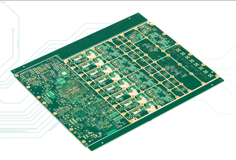
It is a professional R & D and manufacturer of high-precision PCB circuit boards. It can mass produce 4-46 layers of PCB boards, circuit boards, circuit boards, high-frequency boards, high-speed boards, HDI boards, PCB circuit boards, high-frequency high-speed boards, IC packaging carrier boards, semiconductor test boards, multilayer circuit boards, HDI circuit boards, mixed voltage circuit boards, high-frequency circuit boards, soft and hard combination boards, etc.