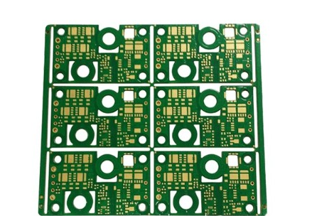
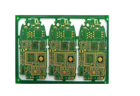
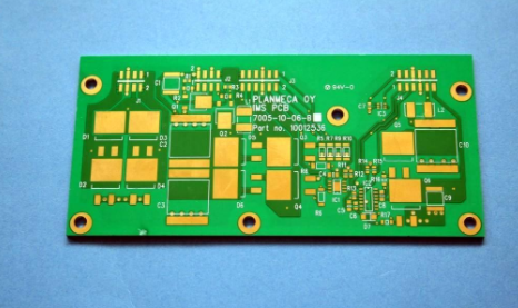
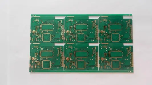
PCB proofing For the most basic PCB, the components are concentrated on one side, and the wires are concentrated on the other side. Because it can only be wired on one side, we call this kind of PCB a single-sided board. Both sides of the double-sided board can be wired, so the wiring area It is twice as large as a single panel and is suitable for use in more complex circuits.

For simple circuits such as radios, single-sided or double-sided manufacturing is sufficient. However, with the development of microelectronics technology, the complexity of the circuit has greatly increased, and higher requirements have been placed on the electrical performance of the PCB. If single-sided or double-sided boards are used, the circuit volume will be very large, and it will also bring great difficulties to the wiring. In addition, the electromagnetic interference between the lines is not easy to handle, so a multilayer board(the number of layers represents There are several independent wiring layers, usually even numbers).
The advantages of using a multilayer board are: high assembly density and small size; the connection between electronic components is shortened, and the signal transmission speed is improved; it is convenient to wire; for high-frequency circuits, a ground layer is added to make the signal line to the ground form a constant Low impedance; good shielding effect. But the more the number of layers, the higher the cost, the longer the PCB proofing processing cycle, and the more troublesome quality inspection.
Our common computer boards usually use four-layer boards or six-layer boards, but now there are more than 100 layers of practical printed circuit boards. The difference between a six-layer board and a four-layer board is in the middle, that is, the ground layer and the power supply There are two more internal signal layers between the layers, which are thicker than the four-layer board.
Multilayer boards are actually made by laminating and bonding several etched single or double panels. The double panels are easy to distinguish. Looking at the light, except for the wiring on both sides, other places are transparent. Light. For four-layer boards and six-layer boards, because the layers in the PCB are very tightly combined, if there are corresponding marks on the board, there is no good way to distinguish.
Via (VIA)-the "bridge" of the circuit
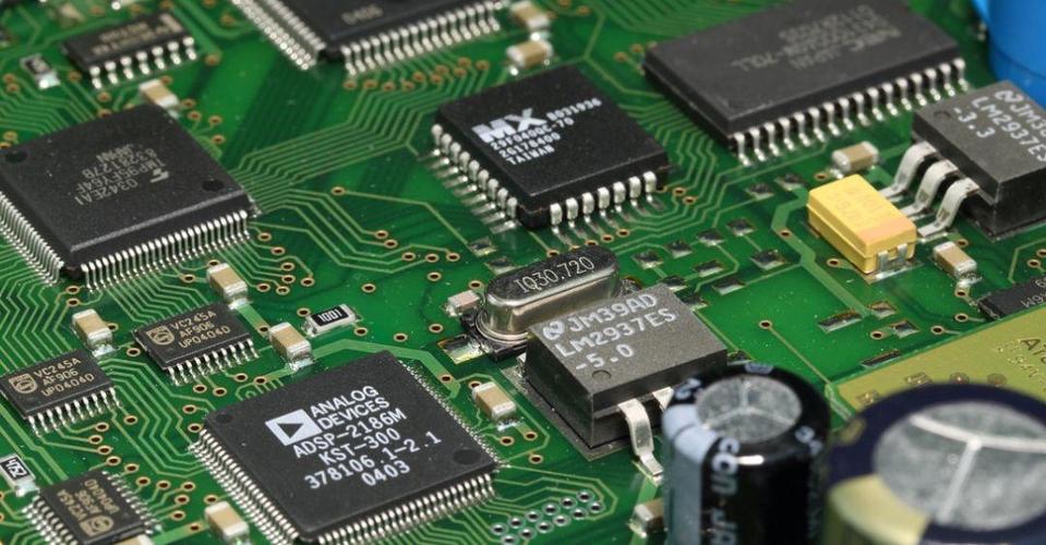
Introduced the multi-layer board, you may have a question in your mind. The layers should be insulated. How does the circuit between them have a relationship? In order to achieve the electrical connection between the layers, the insulation layer of the PCB Holes are punched, and then copper is plated on the wall of the hole to connect the inner and outer layers of the circuit. This kind of hole is called a via, a through hole or a through hole, etc. For multilayer boards, there are several types of vias: through Through-holes in all layers, semi-hidden vias that can only be seen on one side and invisible fully-hidden vias.
In addition to the formation of vias by electroplating, the method of filling "conductive paste" in the voids to make vias has recently become popular. Conductive paste is a paste in which metal particles are added to the resin, and once it is solidified, the metal particles are filled into the hole. If they touch each other, the circuit can be connected. The holes formed in this way are called metal vias, and the holes formed by the silver particle conductive paste are called "silver vias". Recently, copper particles of conductive paste have also been used.
It can be seen that the vias are the "bridges" connecting the circuits, but the "bridges" can't be built randomly. For the connection between two points, too many vias will lead to a decrease in reliability.
The knowledge of wiring
Misunderstandings of Snake Line
A description similar to this can be seen in the trial reports of many boards: "The workmanship is good, and there are many snakes on the board." Maybe everyone's understanding of wiring starts from the snakes, so what exactly is the snake? What's going on?
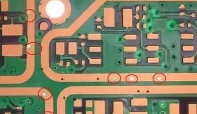
The meandering line usually refers to the kind of wiring that shows a continuous S-shaped change. Intuitively, there is no obstruction between the two points that need to be connected. It could be laid out in a straight line, but the snake wiring is actually used. In theory, the serpentine line has these functions: forming a tiny inductance to suppress the change of the signal current on the line; ensuring the equal length of certain lines; suppressing crosstalk to a certain extent. It can be seen that this is only a partial The designer should adopt the wiring method according to the actual situation, and the quality of the PCB wiring cannot be judged by the number of snaking lines.
Different thickness
When observing the PCB, we will find that the traces are thick and thin. The thick places are usually the power line and the ground line, and the thinner is the data line. This is because the power line and the ground line have to pass a relatively large current, so you should do your best It may be thicker. Therefore, the vacant area is often covered by a piece of copper foil as a ground wire. The current passing through the data line is small, so it can be designed to be thinner, and the thin wire is also more conducive to wiring.
Be careful about turning
The traces on the PCB cannot be all straight lines, so the problem of steering is involved. The design usually requires the traces to be not at right angles when turning, but at a 45 degree angle (referring to the angle between the extension direction of the line). This is because right-angle and acute-angle patterns will affect the electrical performance in high-frequency circuits, and they are easy to peel off at high temperatures, so it is usually required that the turning point of the trace be obtuse or rounded.