Usually what we show on PCB board, the power distribution system (PDS) refers to the subsystem that distributes the power of the Power Source to the devices and devices in the system that need to be powered. There is a power distribution system in all electrical systems, such as the lighting system of a building, an oscilloscope, a PCB board, a package, and a chip, all of which have a power distribution system inside.
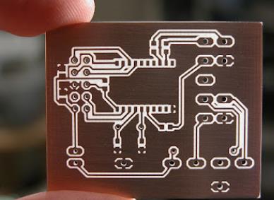
Power distribution system on PCB
In a typical product, the power distribution system includes all interconnects from the voltage regulation module (VRM) to the PCB board, the package, and the chip. It can be divided into four sections: voltage regulation module (VRM) including its filter capacitor - power supply; Bulk capacitor on PCB board, high frequency decoupling capacitor, interconnection line, via, power/ground plane - PCB board power distribution system on the package; package pins, bond wires, interconnects and embedded capacitors - power distribution system on the package; on-chip interconnects and capacitors, etc. - the power distribution system on the chip. The so-called power distribution system on the PCB refers to a system on the PCB that distributes the power of the Power Source to various chips and devices that need to be powered. This article mainly focuses on the power distribution system on the PCB board, so we agree that the power distribution system or PDS mentioned below refers to the power distribution system on the PCB board. The role of the power distribution system is to transmit correct and stable voltage, which means that the voltage at all positions on the PCB can be maintained correct and stable under any load conditions. The study of the correct and stable operation of a power distribution system is what we call the power integrity problem.

Power integrity
The so-called power integrity refers to the degree of compliance of the system power supply with the working power requirements at the device port that needs power supply relative to the device port after passing through the power distribution system. Generally speaking, the devices that need power supply on the PCB board have certain requirements for the working power supply. Taking the chip as an example, it usually shows three parameters: Limit power supply voltage: It refers to the limit power supply voltage that the power supply pins of the chip can withstand. . The power supply voltage of the chip cannot exceed the required range of this parameter, otherwise it may cause damage to the chip; within this range, the function of the chip is not guaranteed; if the chip is at the limit value of this parameter for a certain period of time, it will affect the chip long-term stability; recommended working voltage: refers to the range within which the voltage of the power supply pins of the chip needs to be guaranteed to make the chip work normally and reliably, usually expressed as "V±x%", where V is the typical value of the power supply pins of the chip Working voltage, x% is the allowable voltage fluctuation range, the common x is 5 or 3; power supply noise: refers to the allowable ripple noise on the voltage of the power supply pins of the chip to make the chip work normally and reliably, usually using its peak-to-peak value to characterize. The datasheet of the chip usually provides the requirements for "limit power supply voltage" and "recommended operating voltage". For "power supply noise", it may not be provided separately. In this case, it may be included in the parameter "recommended operating voltage". And "power supply noise" is the focus of this article, and will be discussed separately later. Taking the above example to illustrate, the problem of power integrity is to discuss the "limit power supply voltage" and "recommended working voltage" of the power supply at different power supply pins of the chip relative to the chip pins after the system power supply passes through the power distribution system. ” and “power supply noise” requirements.
Three characteristics of power distribution system
The physical media of the power distribution system are various, including Connector, cable, Trace, Power Plane, GND Plane, Via, Pad, chip pins, etc., and their physical characteristics (material, shape, size, etc.) are different. Since the purpose of the power distribution system is to supply the power of the system power supply to the devices that need to be powered, to provide a stable voltage and a complete current loop, we only focus on three electrical characteristics of the power distribution system: resistance characteristics, inductance characteristics and capacitance characteristics .
Resistance characteristics
Resistance is a physical quantity that characterizes the resistance of a conductor to DC current, usually represented by R. Its main physical feature is that when a current I flows, it converts electrical energy into heat energy (I2R) and produces a DC voltage drop (IR) across it. ). Is a physical property of a conductor and is temperature dependent, the resistivity of a metal generally increases with temperature. Resistance exists everywhere in the power distribution system: DC resistance and contact resistance exist in cables and connectors, distributed resistance exists in copper wires, power supply layers, ground layers, and vias, and DC resistance exists in solder, pads, and chip pins. There is contact resistance between them. IR Drop: This effect causes the power supply voltage to gradually decrease along the power distribution network, or the voltage of the reference ground rises, which reduces the voltage at the port of the device that needs to be powered, causing power integrity problems; Thermal Power Dissipation: This effect reduces the power supply The power is converted into heat, and at the same time, it causes the system temperature to rise, jeopardizing the stability and reliability of the system. The voltage drop IRS on RS reduces the output voltage Voutput of the power supply, the voltage drop IR1 on the power path reduces the supply voltage Vcc of the load, and the voltage drop IR2 on the return path raises the GND level of the load. The voltage drops of the above-mentioned resistors RS , R1 , and R2 will all lead to the reduction of the power supply voltage VCC-GND of the load, and cause the problem of power integrity. The heat loss generated by the resistance of the power distribution system will cause the power of the power supply to be converted into heat and dissipated in vain, thereby reducing the efficiency of the system. At the same time, heating will cause the temperature of the system to rise, reducing the life of some devices (such as electrolytic capacitors) and thus affecting the stability and reliability of the system. Excessive current density in some areas will also cause local temperature to continue to rise or even burn out. It can be seen from the above analysis that these two effects are harmful to the system, and their influence is proportional to the resistance value of the resistance, so reducing the resistance characteristics of the power distribution system is one of our design goals.
Inductance characteristics
Inductance is a physical quantity that characterizes the resistance of a conductor to an alternating current. When a current flows through the conductor, a magnetic field will be formed around the conductor. When the current changes, the magnetic field will also change, and the changing magnetic field will form an induced voltage at both ends of the conductor. The polarity of the voltage will cause the induced induction The current hinders the change of the original current; when the current change in other conductors around the conductor causes the magnetic field around the conductor to change, an induced voltage will also be generated in the conductor, and the polarity of the voltage will cause the induced current to hinder the original current. The change. The effect of this conductor to hinder the current change is called inductance, the former is called self-inductance L, and the latter is called mutual inductance M. Here we directly give two properties of mutual inductance: symmetry: two conductors a and b, regardless of size, shape and relative position, the mutual inductance of conductor a to conductor b is equal to the mutual inductance of conductor b to conductor a, that is, mutual inductance is equally common to both conductors; mutual inductance is less than self-inductance: the mutual inductance of any two conductors is less than the self-inductance of either conductor. This induced voltage caused by current changes is significant in signal integrity (including power integrity) and can cause transmission line effects, abrupt changes, Crosstalk, SSN, Rail Collapse, Ground Bounce and most EMI. In the power distribution system, inductance is ubiquitous. Connectors, cables, copper wires, power layers, ground layers, vias, pads, chip pins, etc. all have inductance, and there is mutual inductance between conductors that are close to each other. Assuming that the local self-inductance of branch a is La, the local self-inductance of branch b is Lb, the local mutual inductance between these two branches is M, and the current in the loop is I. Since the two branches are parallel and the currents flow in opposite directions, the magnetic fields generated by them are in opposite directions. Assuming that I increases, for branch a, the polarity of the induced voltage generated by La will hinder the I in branch a. increase, but the polarity of the induced voltage generated by M will help the increase of I in branch a. If branch a represents the power path and branch b represents the return path, Va represents the power noise (rail collapse/power bounce) on the power path, and Vb represents the track collapse/ground bounce noise on the return path. Both of these two kinds of noise will cause instability of the power supply voltage and cause power integrity problems. Therefore, one of our design goals is to reduce the above two voltages. There are two ways: reduce the rate of change of the loop current as much as possible: This means that the sudden change speed of the current drawn by the load needs to be reduced, the number of power supply ports that share the power supply path and the return path must be limited; The local mutual inductance between the two branches. Reducing the local self-inductance of the branch means using the shortest and widest power path and return path as possible. Increasing the local mutual inductance means that the two branches need to be parallel. And as close as possible under the premise of reverse. From the above analysis, it can be seen that the induced voltage caused by the inductance when the current changes is the source of many problems in the power integrity, so reducing the above-mentioned induced voltage of the power distribution system is one of our design goals.
Power distribution system is the main object of discussion in this paper, and the related content of its work is the issue of power integrity. The power distribution system has resistive, inductive and capacitive characteristics, respectively. Resistive and inductive characteristics are detrimental to power integrity, while capacitive characteristics are beneficial to power integrity. Our design goal is to reduce or even eliminate the influence of resistive and inductive characteristics, and to enhance the influence of capacitive characteristics on PCB board.