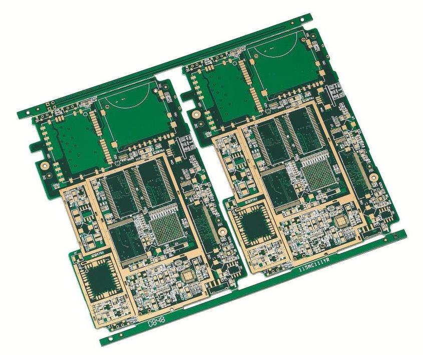
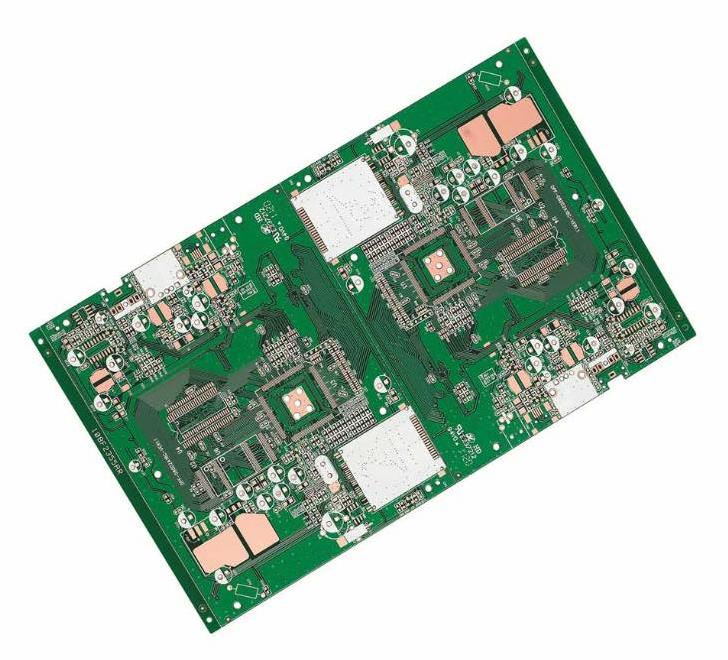
Although EDA tools are now powerful, with the smaller and smaller PCB board size requirements and the higher device density, the difficulty of PCB board design is not small. In order to solve the design difficulties and speed up the listing of products, many manufacturers now tend to use special EDA tools to realize the design of PCB boards. But dedicated EDA tools don't produce the desired results, don't achieve 100% routing, are messy, and often take a lot of time to do the rest. There are many popular EDA tool software on the market now, but they are all the same except for the terms used and the location of the function keys. How do use these tools to better realize the design of the PCB board? Careful analysis of the design and careful setup of the tool software before starting routing will make the design more compliant. Below is the general design process and steps.

1. Determine the number of layers of the PCB board
Board size and routing layers need to be determined early in the design. If the design calls for the use of high-density ball grid array (BGA) components, the low number of routing layers required for routing these devices must be considered. The number of wiring layers and the stack-up method directly affect the wiring and impedance of the traces. The size of the board helps determine the stack-up and trace width to achieve the desired design effect. For many years, it has been assumed that fewer layers are cheaper, but there are many other factors that affect the cost of manufacturing a circuit board. In recent years, the cost differential between multilayer boards has been greatly reduced. Start the design with more circuit layers and evenly distribute the copper to avoid being forced to add new layers when a small number of signals do not meet the defined rules and space requirements until near the end of the design. Careful planning before design will reduce a lot of hassle in wiring.
2. Design Rules and Limitations
The auto-routing tool itself doesn't know what to do. To accomplish routing tasks, routing tools need to work within the correct rules and constraints. Different signal lines have different wiring requirements. It is necessary to classify all signal lines with special requirements, and different design classifications are also different. Each signal class should have a priority, and the higher the priority, the stricter the rules. Rules related to trace width, number of vias, parallelism, the interaction between signal lines, and layer limitations have a large impact on the performance of routing tools. Careful consideration of design requirements is an important step in successful routing.
3. Layout of components
To streamline the assembly process, design for manufacturability (DFM) rules place constraints on component placement. If the assembly department allows the components to move, the circuit can be properly optimized for easier automatic routing. The rules and constraints you define affect the layout design. Routing channels and via areas need to be considered during layout. These paths and areas are obvious to the designer, but the auto-routing tool only considers one signal, and by setting routing constraints and setting the layers on which signal lines can be routed, the routing tool can be made to behave as the designer envisions it. Complete wiring.
4. Fan-out design
In the fan-out design phase, to allow automated routing tools to connect component pins, surface mount devices should have at least one via per pin so that the board can make interlayer connections when more connections are required. Connection, In-Circuit Test (ICT), and circuit reprocessing. In order to make the automatic routing tool efficient, be sure to use the size of the vias and traces as much as possible, and the interval is ideally set to 50mil. The type of via to use that makes the number of routing paths available. When designing a fan-out, consider the problem of in-circuit testing. Test fixtures can be expensive and are often ordered near full production when it is too late to consider adding nodes for 100% testability. After careful consideration and prediction, the design of the circuit in-circuit test can be carried out in the early stage of design and realized in the later stage of the production process. The type of via fan-out is determined according to the wiring path and circuit in-circuit test. Power and grounding will also affect the wiring and fan-out design. . In order to reduce the inductive reactance generated by the connection lines of the filter capacitors, the vias should be as close as possible to the pins of the surface mount device, and manual routing can be used if necessary, which may affect the originally envisaged routing path, and may even cause you to re- Considering which via to use, the relationship between via and lead inductance must be considered and the via specification prioritized.
5. Manual wiring and processing of key signals
Although this article focuses on automatic routing issues, manual routing is and will be an important process in printed circuit board design. Using manual routing helps automatic routing tools to complete routing work. As shown in Figures 2a and 2b, by manually routing and fixing the selected nets, a path that can be followed during automatic routing can be formed. Regardless of the number of critical signals, route those signals first, either manually or with automated routing tools. Critical signals often require careful circuit design to achieve the desired performance. After the wiring is completed, the relevant engineering personnel will check the signal wiring, which is much easier. Once the inspection passes, the wires are secured and the auto-routing of the remaining signals begins.
6. Automatic wiring
The routing of key signals needs to consider controlling some electrical parameters during routing, such as reducing distributed inductance and EMC, etc. The routing of other signals is also similar. All EDA vendors provide a way to control these parameters. After understanding the input parameters of the automatic routing tool and the influence of the input parameters on the routing, the quality of the automatic routing can be guaranteed to a certain extent. General rules should be used for the automatic routing of signals. By setting constraints and no-routing areas to limit the layers used for a given signal and the number of vias used, the routing tool can automatically route according to the engineer's design thinking. If there is no limit to the layers used by the auto-routing tool and the number of vias routed, each layer will be used during auto-routing and many vias will be created. Once the constraints are set and the rules created are applied, auto-routing will achieve similar results as expected, although some tidying may be required, as well as ensuring room for other signals and network routing. After a portion of the design is complete, it is secured to protect it from subsequent routing processes. Use the same steps to route the remaining signals. The number of traces depends on the complexity of the circuit and how many general rules you have defined. After each type of signal is completed, the constraints on the routing of the remaining nets are reduced. But with that comes a lot of signal routing that requires manual intervention. Today's auto-routing tools are very powerful and often do 100% of the routing. However, when the automatic routing tool does not complete the routing of all signals, the remaining signals need to be manually routed.
7. The design points of automatic wiring include:
7.1 Slightly change the settings and try a variety of path wiring;
7.2 Keep the basic rules unchanged, try different wiring layers, different printed lines and spacing widths, different line widths, different types of vias such as blind vias, buried vias, etc., and observe how these factors affect the design results;
7.3 Let the routing tool process those default nets as needed;
7.4 The less important the signal, the more freedom the auto-routing tool has to route it.
8. Arrangement of wiring
If the EDA tool you are using can list the routing lengths of the signals, check this data and you may find that some signals with few constraints have very long routing lengths. This problem is relatively easy to deal with, and manual editing can shorten the signal routing length and reduce the number of vias. During the sorting process, you need to determine which wiring is reasonable and which is not. Like manually routed designs, auto routed designs can also be organized and edited during the review process.
9. The appearance of the circuit board
The previous design often paid attention to the visual effect of the circuit board, and now it is not the same. An automatically designed PCB board is not as aesthetically pleasing as a manual design but meets the specified requirements in terms of electronic characteristics, and the complete performance of the design is guaranteed.