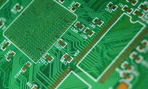
Antenna PCB wireless devices have been widely used in telecommunications to receive and transmit signals. With the advent of 5G networks,more and more electronic devices need antenna PCB communication,known as the Internet of Things (IoT).

PCB board antenna refers to the part of PCB board used for wireless reception and transmission. When transmitting,it converts the high frequency current of the transmitter into space electromagnetic wave; When receiving,it converts the electromagnetic wave intercepted from space into high-frequency current and sends it to the receiver. Its advantages are: less space occupation,low cost,no need to separately assemble the antenna,it is not easy to touch and damage,and it is convenient to assemble the whole machine,but there are gains and losses-sacrificing performance. Disadvantages: single antenna field is difficult to achieve roundness,high insertion loss, relatively low efficiency,and vulnerable to interference on the motherboard. The antenna PCB board material should have high frequency,and generally FR4 canot has good performance. Here we list the materials that can be used to manufacture antenna PCB: Rogers PCB,Teflon,Arlon,Taconic,Nelco,FR4, Dupont,Isola. The ultimate purpose of the antenna is to radiate RF signals into the free space. At this time,the design of the antenna is very important. However,the antenna design largely depends on the characteristics of the installed platform. In addition,the antenna is very sensitive to the surrounding environment. In many cases,the antenna is a unique design for each platform. As the customer is not clear about the factors considered in the antenna design,here are some suggestions on the design of portable device antennas,which will help the customer better design their own circuits and PCB boards and increase the chances of success of the project. However,each project has its own characteristics,so there are still some problems that need specific analysis.
Design PCB board antenna: antenna PCB design and RF layout are the two most important components of any wireless device. You can use two identical RF products,each with a different PCB antenna design and layout,and obtain two distinct RF performance ranges. What's the difference between them? It all depends on the quality and considerations in the design process. Many electronic applications in the 2.4 GHz and 915 MHz frequency bands used for commercial and consumer purposes require compact PCB board antennas to operate in the ISM band. As the name implies, PCB board antenna is directly printed on the circuit board. Good RF grounding is undoubtedly very important for the wireless performance of mobile phones,and the following design principles must be followed: try to make the ground of the outer area complete and not be broken (the part inside the unshielded cover),which is particularly important for the area near the antenna. The antenna current must be isolated from the noise current. If the grounding area near the antenna is damaged to be incomplete,a filling ground plane must be generated in the relevant area below it and sewed with a ground through hole to make it a complete ground. The wiring in this area must ensure that the antenna current only flows through the surface plane,and must limit the noise current to flow into the complete ground plane inside. When using pre production antennas,it should be noted that their characteristics depend on the connected ground plane. The specifications indicated by the manufacturer can be reached only when the size and shape of the grounding plane are consistent with the manufacturer's evaluation plate. In other cases,users need to measure the impedance of the pre produced antenna under practical application conditions and match it to the required characteristic impedance.
The following aspects mainly affect the performance of GPS antenna:
1) Ceramic chip: the quality of ceramic powder and sintering process directly affect its performance. The ceramic chips currently used in the market are mainly 25×25、18×18、15×15、12×12. The larger the area of ceramic sheet,the larger the dielectric constant,the higher the resonance frequency,and the better the acceptance effect. Most of the ceramic chips are square in design to ensure that the resonance in the XY direction is basically consistent, so as to achieve the effect of uniform star collection.
2) Silver layer: The silver layer on the surface of ceramic antenna can affect the resonant frequency of antenna. The ideal frequency point of GPS ceramic chip is accurate at 1575.42MHz, but the antenna frequency point is very vulnerable to the surrounding environment. Especially when it is assembled in the whole machine, the frequency point must be adjusted to maintain 1575.42MHz again by adjusting the shape of the silver coating. Therefore, when purchasing antenna,the manufacturer of GPS complete machine must cooperate with the antenna manufacturer to provide complete machine samples for testing.
3) Feed point: the ceramic antenna collects the resonance signal through the feed point and sends it to the rear end. Because of antenna impedance matching, the feed point is generally not in the center of the antenna,but slightly adjusted in the XY direction. This impedance matching method is simple and does not increase the cost. Moving only in the single axis direction is called monopolarized antenna, and moving in both axes is called bipolarized antenna.
4) Amplification circuit: shape and area of PCB board carrying ceramic antenna. Because GPS has the characteristic of touchdown rebound,when the background is 7cm×7cm, the performance of the patch antenna can be maximized. Although restricted by such factors as appearance and structure,try to maintain a considerable area and uniform shape. The gain of the amplifier circuit must be selected in conjunction with the rear LNA gain. The GSC3F of SiRF requires that the total gain before signal input shall not exceed 29dB,otherwise the signal over saturation will generate self excitation on antenna PCB.