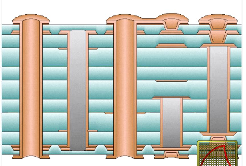
One of the more easily forgotten themes in PCB design is the holes for mounting components. Specify the tolerance of hole size in PCB manufacturing to ensure the correct fit of plated through hole (PTH) components.
Altium Designer PCB design software can add hole tolerance attributes for your pads and through holes, which will be transferred to the manufacturer by including them in the drill table. Here are five tips to help you quickly specify the hole size in the next PCB design.
PCB tolerance
The component data book lists the plus/minus tolerances to accommodate changes in aging, wear, temperature, plating, materials, processing, etc. For example, the 1/4 watt resistor manufacturer's data sheet specifies a wire diameter of 0.022 ± 0.003. Therefore, the actual diameter can vary from 0.019 to 0.025.
Normally the PCB manufacturer specifies a hole tolerance of ± 0.004. Whether at the big end or the small end of the tolerance zone, the wire must always be stuck in the hole. Therefore, the minimum hole size must accommodate the maximum resistance lead plus tolerance (0.022 resistance lead+0.003 resistance lead tolerance), plus 0.004 PCB hole tolerance. Therefore, 0.022+0.003+0.004=0.029 inch, which is the minimum allowable hole size on the plate.
When drilling, the bit wear becomes smaller. Alternatively, the drill bit may vibrate or shake slightly in the hole, resulting in a slightly larger hole. The holes are then plated, and the plating can be thicker or thinner for each batch or location on the plate. You must also consider the thermal expansion or contraction of the PCB substrate during processing.

Therefore, the hole tolerance is critical in the design process to ensure the correct placement of PTH parts. As a rule of thumb, you should make PCB holes 0.007 inches larger than the part wire diameter to accommodate all tolerances, drill wear or wobble, and plating changes. There is no default hole tolerance in Altium Designer. You can adjust hole tolerance attributes in the Pads and Attributes dialog box. Hole tolerances and default values can also be established in the Pad Via Library panel and Footprint Library.
5 Tips for Specifying PCB Hole Tolerance
The hole tolerance in Altium Designer can be accessed and edited in several different ways, which we will study below. In each method, you can set the minimum (-) and maximum (+) hole tolerance attributes.
You can quickly set pad/through-hole tolerances based on individual attributes.
Right click a pad or through hole and select Properties. In the Pad Properties dialog box (Figure 1), edit the hole tolerance at Hole Information.
In the Through Hole Properties dialog box, edit the hole tolerance at Tolerance in the upper left corner of Figure 2.
Tips for Specifying PCB Hole Tolerance
You can also specify hole tolerances using pads or through hole templates.
Right click Pad Via Library and select Add Through Hole Template or Add Pad Template. The hole tolerance can be set at Hole Information.
Conveniently, you can set the hole tolerance of multiple pads or through holes at the same time.
Open the PCB Inspector panel, as shown in Figure
3. Select the pad or through hole on the PCB you want to set, and enter the required hole metric value in the right column under the Object Specific panel.
Tips for Specifying PCB Hole Tolerance
Hole tolerance bars can also be added and edited from the PCB panel using the Hole Size Editor. Right click Columns>Hole Tolerance (+) and Hole Tolerance (-) under the Unique Holes heading. You can change the tolerance attributes by clicking in the Hole Tolerance column.
Tips for Specifying PCB Hole Tolerance
You can add hole tolerances for multiple stitched through holes to save time.
Click "Tools">"Via Stitting/Shielding">"Add Stitting to Net". Add hole tolerance information at Tolerance under the Via Style section.
Tips for Specifying PCB Hole Tolerance
You can view the tolerances in the drilling table in two ways: one or two columns to display the tolerance attributes.
In the Drill Table Properties dialog box, click Add Column. Select Hole Tolerance to view all the tolerance attributes in a column, and select Hole Tolerance. This column displays the minimum and maximum properties. Alternatively, you can choose to display the Min and Max setup hole tolerance attributes in separate columns. For the latter selection, select Hole Tolerance (+) and Hole Tolerance (-). Of course, you can also choose to display only the minimum or maximum set hole tolerances.
Tips for Specifying PCB Hole Tolerance
Table 1 Example table showing all hole tolerance columns
You can also group them by hole tolerance. From the Drill Symbols dialog box (click Configure Drill Symbols in the Drill Table dialog box), click Grouping, and then select Hole Tolerance.
Note that when hole tolerance information is added to pads and through holes, unless all pads or through holes grouped under the "Count column" column have the same hole tolerance attribute, the hole tolerance value will be displayed as * (asterisk).
Note: After adding information to the drill table, you must click OK to exit the Drill Table dialog box, or your changes will not be saved.
conclusion
Ensuring proper hole tolerance is critical for the PTH components to be correctly installed on the PCB design. Altium Designer simplifies the documentation of your hole size tolerances so that your tolerance specifications can be easily communicated to your manufacturers.