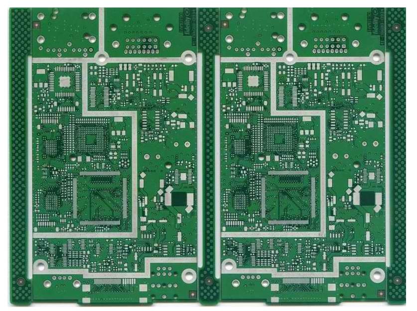
Pre coat a layer of lead tin anti-corrosive layer on the copper foil to be retained on the PCB board, and then chemically etch the rest of the copper foil, which is called etching. Then, what are the types of PCB etching and the commonly used etchants?

1. Types of PCB etching
1) Pattern electroplating method: when etching, there are two layers of copper on the board, only one layer of copper is completely etched, and the rest will form the final required circuit.
2) Full plate copper plating process: the whole plate is copper plated, and the parts outside the photosensitive film are only tin or lead tin corrosion resistant layers. Compared with pattern electroplating, its biggest disadvantage is that copper must be plated twice everywhere on the board, and they must be corroded when etching.
3) A photosensitive film is used as an anti-corrosion layer instead of a metal coating. This method is similar to the inner layer etching process.
4) The photochemical etching process applies layers of photoresist or anti-corrosion dry film on the clean copper clad plate, and obtains the power circuit image according to the exposure, development, film fixation and etching process of the photographic base plate. After the film is removed, it is mechanically processed, coated on the surface, and then packaged, printed and marked into finished products. This kind of processing technology is characterized by high precision graphics, short manufacturing cycle time, and suitable for batch production and multi category production.
5) The stencil prepared in advance with the power circuit pattern required is placed on the copper surface layer of the clean copper clad plate by the wire mesh leak printing etching process, and the anti corrosion raw materials are leak printed on the copper foil surface layer by the scraper to obtain the print pattern. After drying, the organic chemical etching process is carried out to remove part of the bare copper that is not covered by the printing material, and finally the printing material is removed, which is the required power circuit pattern. This kind of method can carry out large-scale professional production and manufacturing, with large production volume and low cost, but its precision is not comparable to that of chemical etching process.
6) Rapid etching process for ultra-thin copper foil removal: This etching process is mostly applied to thin copper foil laminates. The processing technology is similar to the pattern electroplating and etching process. Only after the pattern is plated with copper, the thickness of a part of the power circuit pattern and the metal material copper at the hole edge is about 30 μm, the copper removal foil that is not part of the power circuit figure is still thin (5 μm)。 It was quickly etched, 5μm part of the m-thick non power circuit has been etched, leaving only a small part of the etched power circuit pattern. This kind of method can produce high-precision and dense printed circuit boards, which is a new production process with a promising future.
2. What are PCB board etchants
Ammonia etchant is a commonly used chemical solution, which does not have any chemical reaction with tin or lead tin. In addition, there is ammonia water/ammonia sulfate etching solution. After use, copper in it can be separated by electrolysis; It is generally used in chlorine free etching. Others use sulfuric acid hydrogen peroxide as an etchant to etch the outer figure, which has not been widely used.
In the transmission signal line of electronic devices, the resistance encountered in the transmission of high-frequency signals or electromagnetic waves is called impedance. Why must PCB be impedance in the manufacturing process? Let's analyze the following four reasons:
1) PCB board shall consider the connection and installation of electronic components, and the later SMT patch connection shall also consider the conductivity and signal transmission performance, so the lower the impedance, the better.
2) During the production process of PCB board, the process of copper deposition, electro tin plating (or chemical plating, thermal spraying tin), connector soldering and other production links are involved. The materials used must have low resistivity to ensure that the overall impedance value of PCB board meets the product quality requirements and can operate normally.
3) The tin plating of PCB is the most likely problem in the whole PCB production, and is the key link affecting the impedance; Its biggest defect is easy oxidation or deliquescence, poor solderability, which makes the circuit board difficult to weld, high impedance, resulting in poor conductivity or unstable performance of the whole board.
4) The conductor in the PCB will have various signals transmitted. The impedance value of the circuit itself will change due to different factors such as etching, stack thickness, and wire width, which will distort the signal and lead to the decline of the PCB board performance. Therefore, it is necessary to control the impedance value within a certain range.