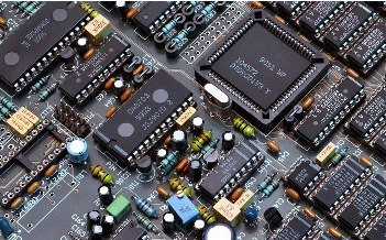
Five precautions for PCBA proofing
Many electronic product companies focus on design, R&D, and marketing, and fully outsource electronic manufacturing. From product prototype design to market launch, there are many development and testing cycles, of which sample testing is extremely critical. Delivering the designed PCB file and BOM list to the electronics manufacturer, it is also necessary to analyze from multiple angles to ensure that there is no delay in the project cycle and reduce the risk of product launch
First, it is necessary to analyze the market positioning of the electronic products developed, and different market strategies determine different product development. If it is a high-end electronic product, the material must be strictly selected in the sample stage, the packaging process must be ensured, and the real mass production process must be simulated 100% as much as possible. If it is a very common electronic product, and the plan is mature, then it can be accepted in the sample stage, such as using some substitute materials, expanding the acceptance range of ICT testing, and so on.
Second, PCBA processing sample production must follow the principle of speed higher than cost. It usually takes 5-15 days from the design plan to the return of the PCBA samples. If the control is not good, this time may be extended to 1 month. If there is a time delay caused by human factors, it will have a great negative impact on the project schedule. In order to ensure that we can receive PCBA samples within the fastest 5 days, we need to start choosing electronics manufacturing suppliers (with process capability, good coordination, and focus on quality and service) during the design stage, and we can even pay 50% more for proofing cost.

Third, the design plan of the electronic product design company must follow the specifications as much as possible, such as the reservation of the circuit board design heat dissipation hole, the marking of the silk screen, the normalization of the materials in the BOM list, the clear marking, and the clear remarks on the process requirements in the Gerber file, etc. Wait. This can greatly reduce the time to communicate with electronics manufacturers, and can also prevent erroneous production caused by unclear design schemes.
Fourth, fully consider the risks in the logistics and distribution links. In PCBA packaging, electronics manufacturers are required to provide safety packaging, such as bubble bags, pearl cotton, etc., to prevent collisions and damage in logistics.
Fifth, when deciding the quantity of PCBA proofing, adopt the principle of maximization. General project managers, product managers, general managers, and even marketing personnel may need prototypes. In addition, it is necessary to fully consider the burn-in during the test. Therefore, it is generally recommended that the proofing is more than 10 yuan.
PCBA production is based on quality and speed, and good communication with electronics manufacturers is the catalyst. When an electronic product company has such a concept, it can gradually form a stable cooperative relationship and good design habits to maximize the smooth progress of the project.